
V1

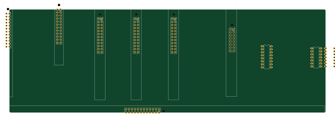
About the V1 PCB
V1 is an open source PCB design by lorenzonotaro, published on GitHub. It is a 2-layer board measuring 266.6 × 86.9 mm, with 10 components from 10 distinct parts.
Other key parts include the RB, RC, RD, 74HC138 and LNCPU ALU Operand Selector.
From the project
v1 is the current implementation of the lncpu.
v1 is the current implementation of the lncpu.
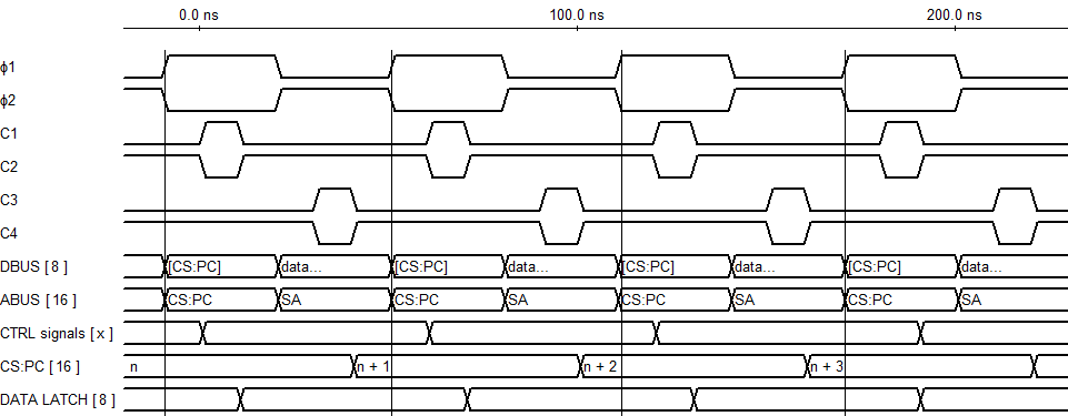
The clock cycle is divided in two phases: Φ1 (control phase) and Φ2 (data phase).
During Φ1, the data bus contains the contents of [CS:PC]: only the device mapped to the memory section containing address CS:PC` is allowed to write to the data bus, regardless of control signals.
* During Φ2, bus control is determined by the control signals of the current microinstruction.
Main components on the V1
V1 bill of materials (BOM)
10 components, 10 distinct parts.
| Qty | Part | Footprint | Refs |
|---|---|---|---|
| 1 | RB | LNCPU_GP_Register | U1 |
| 1 | RC | LNCPU_GP_Register | U2 |
| 1 | RD | LNCPU_GP_Register | U3 |
| 1 | 74HC138 | DIP-16_W7.62mm_LongPads | U4 |
| 1 | LNCPU ALU Operand Selector | LNCPU_Alu_Operand_Selector | U5 |
| 1 | 74LS08 | DIP-14_W7.62mm_LongPads | U6 |
| 1 | 74LS32 | DIP-14_W7.62mm_LongPads | U7 |
| 1 | LNCPU ALU | LNCPU_ALU | U8 |
| 1 | RA | LNCPU_Shift_Register | U9 |
| 1 | LNCPU Type B Connector | LNCPU FLAGS Register | U10 |
V1 design files
The KiCad project lives in the lorenzonotaro/lncpu repository on GitHub; these links point at the commit this page was built from.
- Layoutv1/kicad/v1.kicad_pcb
- Schematicv1/kicad/v1.kicad_sch
V1: common questions
How big is the V1 PCB?
The V1 measures 266.6 × 86.9 mm, has 2 copper layers and is 1.6 mm thick.
How many components are on the V1?
10 components, from 10 distinct parts. The full bill of materials is listed on this page.
Where can I download the V1 design files?
From the lorenzonotaro/lncpu repository on GitHub, which has the KiCad layout and the schematic; the links under Design files point to each one.
Can I use the V1 design in my own project?
The repository has no license, so all rights stay with lorenzonotaro. Use it as a reference, and ask the author before reusing the design.
More boards in lncpu
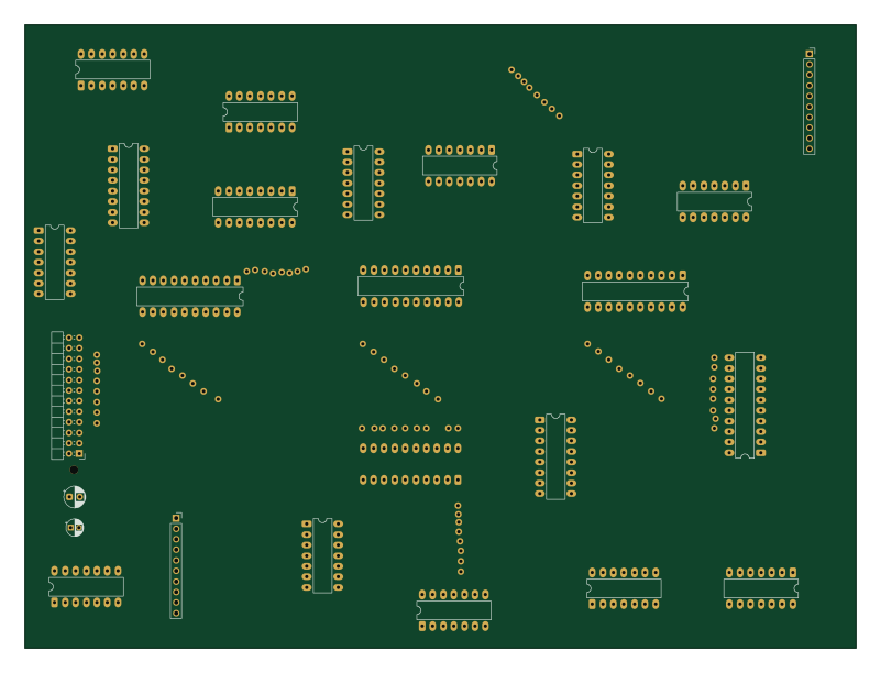
Alu base
200 × 150 mm45 parts2LNo license8
Alu
200 × 150 mm45 parts2LNo license8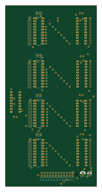
Alu operand selector
82.5 × 163.2 mm29 parts2LNo license8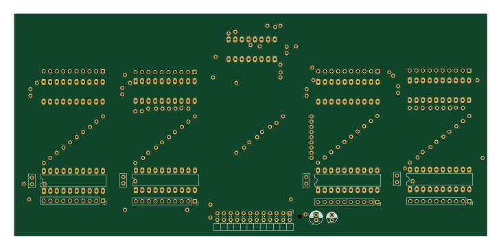
Alu operand selector horizontal
182.2 × 85.5 mm29 parts2LNo license8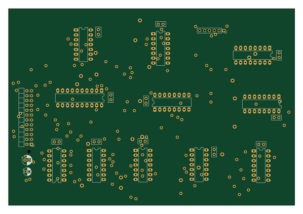
Flags
149.4 × 102.8 mm26 parts2LNo license8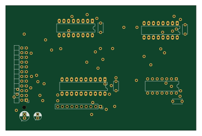
Sp register
101.5 × 66.5 mm12 parts2LNo license8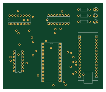 AVR/Arduino
AT28C64B-circuit second sol
90 × 78 mm11 parts2LNo license8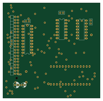
Ram
82.8 × 81 mm11 parts2LNo license8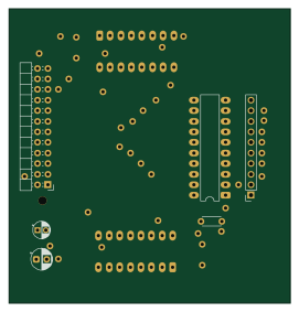
Register
67.5 × 70.6 mm10 parts2LNo license8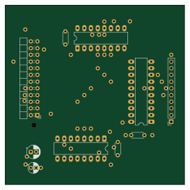
Sh register
68 × 68 mm10 parts2LNo license8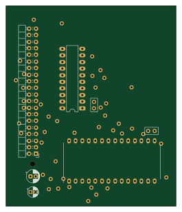
Rom
65.5 × 77 mm7 parts2LNo license8