
Adc cape

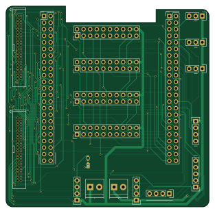
About the Adc cape PCB
Adc cape is an open source PCB design by loxodes, published on GitHub. It is a 4-layer board measuring 78.1 × 77.5 mm, with 22 components from 11 distinct parts.
Other key parts include the boosterpack_ti and 74HC04_FULL. By type, the board carries 16 connectors, 3 ICs, 1 diode, 1 capacitor and 1 resistor.
It belongs with the audio designs in this gallery.
From the project
Under development open hardware microwave vector network analyzer
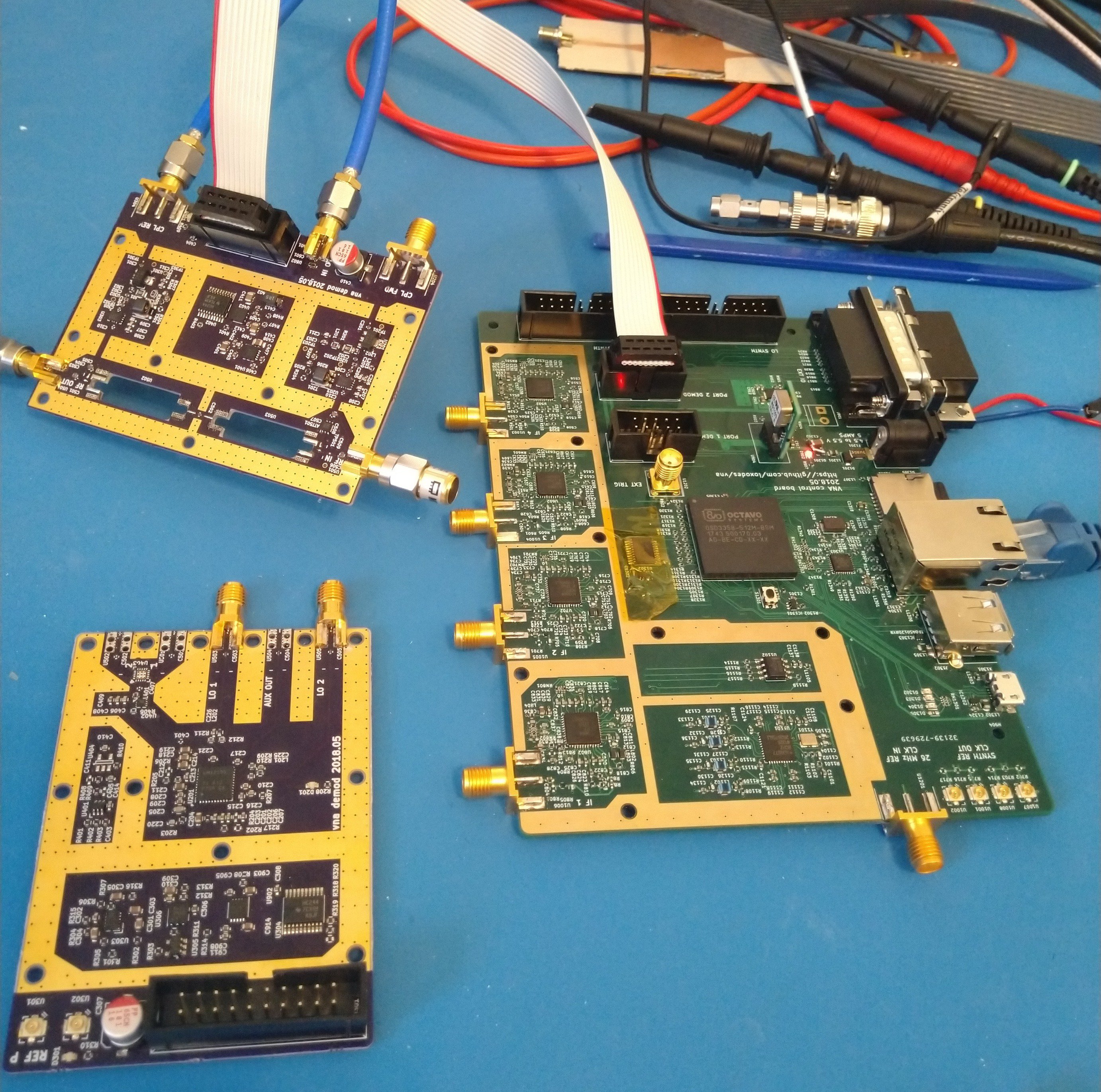
Main components on the Adc cape
Adc cape bill of materials (BOM)
22 components, 11 distinct parts — part numbers from the project's BOM.
| Qty | Part | Footprint | Refs |
|---|---|---|---|
| 2 | boosterpack_ti | 3221-40-0100-00_conn40 | U101, U102 |
| 1 | 74HC04_FULL | TSSOP-14_4.4x5mm_Pitch0.65mm | U103 |
| 2 | CONN_02X23 | Pin_Header_Straight_2x23 | P101, P102 |
| 1 | CONN_01X05 | Pin_Header_Straight_1x05 | P103 |
| 3 | CONN_01X03 | Pin_Header_Straight_1x03 | P105, P106, P107 |
| 4 | CONN_01X04 | Pin_Header_Straight_1x04 | P109, P116, P117, P118 |
| 2 | CONN_01X02 | TerminalBlock_Pheonix_PT-3.5mm_2pol | P110, P111 |
| 4 | CONN_02X10 | Pin_Header_Straight_2x10 | P112, P113, P114, P115 |
| 1 | LED | LED_0603 | D101 |
| 1 | 100 nF | C_0603 | C101 |
| 1 | 10k | R_0603 | R101 |
Adc cape design files
The KiCad project lives in the loxodes/vna repository on GitHub; these links point at the commit this page was built from.
Adc cape: common questions
How big is the Adc cape PCB?
The Adc cape measures 78.1 × 77.5 mm, has 4 copper layers and is 1.6 mm thick.
How many components are on the Adc cape?
22 components, from 11 distinct parts, with part numbers taken from the project's own BOM. The full bill of materials is listed on this page.
Where can I download the Adc cape design files?
From the loxodes/vna repository on GitHub, which has the KiCad layout and the BOM; the links under Design files point to each one.
Can I use the Adc cape design in my own project?
The repository has no license, so all rights stay with loxodes. Use it as a reference, and ask the author before reusing the design.
More boards in vna
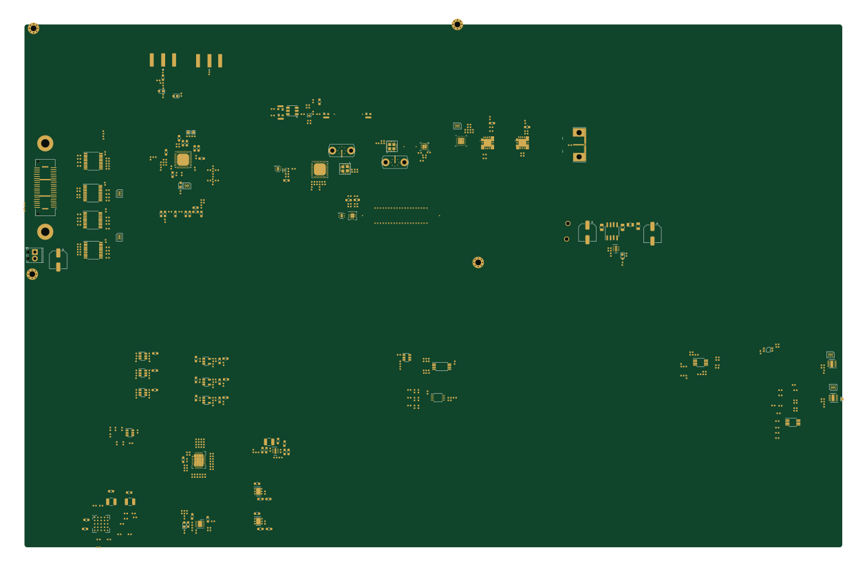
Vna mm synth
314.5 × 201 mm428 parts6LNo license205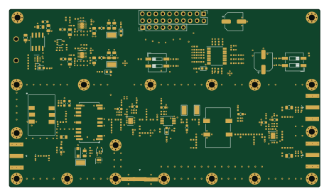
Vna mm ref
115.5 × 66 mm210 parts4LNo license205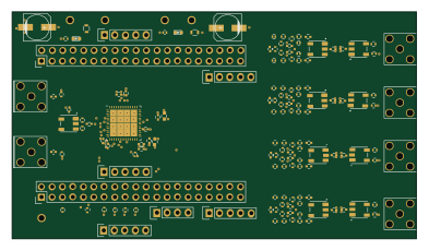
Adc344x
98 × 55 mm161 parts4LNo license205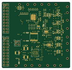
Sequencing ltc2937
58 × 56 mm153 parts4LNo license205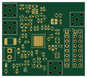
Ad9864 breakout
44 × 39 mm83 parts4LNo license205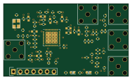
Synth
47 × 27.5 mm80 parts4LNo license205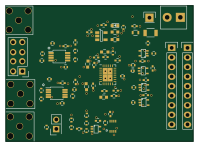
Adc dual
49.8 × 36 mm78 parts4LNo license205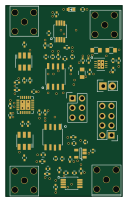
Demod breakout
30.8 × 50.5 mm67 parts4LNo license205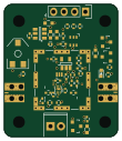
Amp macom vga
27 × 31.5 mm48 parts4LNo license205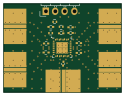
Pe42520 breakout
31.3 × 23.5 mm19 parts4LNo license205
Adrf5020 breakout
29 × 36 mm18 parts4LNo license205
Similar boards
KLOR
GEIGEIGEIST
160.2 × 118.3 mm79 parts2LGPL-3.01.2k
ButtonsLEDs
shanteacontrols
390 × 37 mm82 parts2LApache-2.0956
USB
52 × 12.6 mm6 parts2LApache-2.0956
Pots
390 × 93 mm75 parts2LApache-2.0956
PicoGUS Hand386
polpo
29.2 × 75.2 mm43 parts4LGPL-2.0800
Snark barker
schlae
231.1 × 106.7 mm193 parts2LNo license687