
Fault Latch 2

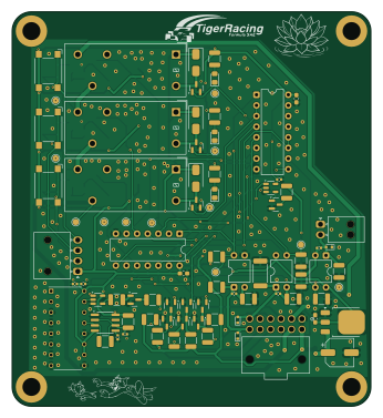
About the Fault Latch 2 PCB
Fault Latch 2 is an open source NXP PCB design by LSUTigerRacing, published on GitHub. It is a 2-layer board measuring 85.8 × 94.2 mm, with 103 components from 52 distinct parts.
Its main chip is the TEENSY4.0, from the NXP family. Other key parts include the CD4027BE, TJA1051T-3, SPAN02A-12, SN74HC00N and 4N35. By type, the board carries 38 resistors, 20 capacitors, 17 transistors, 10 ICs, 9 diodes and 3 connectors.
From the project
This repository contains all of the KiCad Schematics for the 2026 TigerRacing Formula SAE's Electronics Subsystem.
1. Log into GitHub 2. Click your profile picture → Settings 3. Scroll down and click Developer settings (bottom of the left sidebar) 4. Click Personal access tokens → Tokens (classic) 5. Click Generate new token (classic) 6. Give it a name (e.g. git-access), set an expiration, and check the repo scope 7. Click Generate token and copy it — you won't be able to see it again!
Main components on the Fault Latch 2
Fault Latch 2 bill of materials (BOM)
103 components, 52 distinct parts — part numbers from the project's BOM.
| Qty | Part | Footprint | Refs |
|---|---|---|---|
| 1 | CD4027BE | DIP794W53P254L1930H508Q16N | IC1 |
| 1 | TJA1051T-3 74LS279 | DIP-16_W7.62mm | U1 |
| 1 | SPAN02A-12 LM1117DT-5.0 | TO-252-3_TabPin2 | U2 |
| 1 | TEENSY4.0 SFH617A-1 | DIP-4_W7.62mm | U3 |
| 1 | SN74HC00N 74HC00 | DIP-14_W7.62mm | U4 |
| 2 | 4N35 SFH617A-1 | DIP-4_W7.62mm | U5, U6 |
| 2 | LM331 SN74AHC1G08DBVR | SOT-23-5 | U7, U8 |
| 1 | LM555xM | SOIC-8_3.9x4.9mm_P1.27mm | U118 |
| 1 | 2N7002 Q_NMOS_GSD | SOT-23 | Q3 |
| 10 | Q_NMOS_GSD | SOT-23 | Q4, Q105, Q106, Q112, Q113, Q114, Q115, Q117 +2 |
| 6 | Q_NPN_BEC | SOT-23 | Q101, Q102, Q103, Q104, Q110, Q111 |
| 1 | 1053141312 | CONN_SD-105314-100_12_MOL_Nano | J1 |
| 1 | MINI-FIT_JR_5566-04A 4pinNanofit | Molex_Nano-Fit_105313-xx04_1x04_P2.50mm_Horizontal | J2 |
| 1 | 1053131202 | Molex_Nano-Fit_105313-xx02_1x02_P2.50mm_Horizontal | J4 |
| 3 | G2RL-1-DC12 Relay_SPDT_Omron_G2RL-1 | Relay_SPDT_Omron_G2RL-1 | K1, K2, K3 |
| 3 | SW_Omron_B3FS | SW_SPST_Omron_B3FS-100xP | SW101, SW102, SW103 |
| 3 | Bi-TVS Diode | D_SOD-523 | D1, D2, D3 |
| 3 | RED | LED_0805_2012Metric_Pad1.15x1.40mm_HandSolder | D102, D107, D109 |
| 3 | D_Schottky | D_SMA | D104, D108, D110 |
| 1 | 100N 100n | C_0603_1608Metric_Pad1.08x0.95mm_HandSolder | C1 |
Show 32 more
| Qty | Part | Footprint | Refs |
|---|---|---|---|
| 1 | 100N 0.1u | C_0402_1005Metric | C2 |
| 4 | 0.1u | C_0402_1005Metric | C3, C108, C112, C118 |
| 1 | 220U 1u | C_0402_1005Metric | C4 |
| 2 | 220U 0.1u | C_0402_1005Metric | C5, C6 |
| 3 | 10n | C_0603_1608Metric_Pad1.08x0.95mm_HandSolder | C101, C105, C106 |
| 1 | 1u | C_0402_1005Metric | C107 |
| 1 | .01u | C_0402_1005Metric | C109 |
| 1 | 22u | C_0402_1005Metric | C111 |
| 1 | 47u | CP_Elec_6.3x5.4 | C113 |
| 1 | 1u | C_0805_2012Metric_Pad1.18x1.45mm_HandSolder | C114 |
| 1 | 0.33u | C_0603_1608Metric_Pad1.08x0.95mm_HandSolder | C115 |
| 2 | 100n | C_0603_1608Metric_Pad1.08x0.95mm_HandSolder | C116, C117 |
| 1 | 160 10k | R_1210_3225Metric | R1 |
| 1 | 200 1k | R_1210_3225Metric | R2 |
| 1 | 200 270R | R_1210_3225Metric | R3 |
| 1 | 200 10k | R_1210_3225Metric | R4 |
| 1 | 200 2.2k | R_2512_6332Metric | R5 |
| 1 | 20K 1k | R_1210_3225Metric | R6 |
| 1 | 6K8 10k | R_1210_3225Metric | R7 |
| 1 | 10K 1k | R_1210_3225Metric | R8 |
| 1 | 20K 10k | R_1210_3225Metric | R9 |
| 1 | 6K8 510R | R_1210_3225Metric | R10 |
| 1 | 1K5 10k | R_1210_3225Metric | R12 |
| 1 | 12K 510R | R_1210_3225Metric | R13 |
| 7 | 100k | R_1210_3225Metric | R101, R110, R113, R119, R122, R127, R132 |
| 5 | 10k | R_1210_3225Metric | R105, R114, R121, R123, R136 |
| 6 | 1k | R_1210_3225Metric | R108, R111, R115, R120, R124, R129 |
| 1 | 510R | R_1210_3225Metric | R112 |
| 3 | 2k | R_1210_3225Metric | R117, R128, R137 |
| 2 | 270R | R_1210_3225Metric | R130, R150 |
| 1 | 680 | R_1210_3225Metric | R133 |
| 1 | 5.6k | R_1210_3225Metric | R141 |
Fault Latch 2 design files
The KiCad project lives in the LSUTigerRacing/Electronics repository on GitHub; these links point at the commit this page was built from.
Fault Latch 2: common questions
What microcontroller does the Fault Latch 2 use?
The Fault Latch 2 is built around the TEENSY4.0, from the NXP family.
How big is the Fault Latch 2 PCB?
The Fault Latch 2 measures 85.8 × 94.2 mm, has 2 copper layers and is 1.600198 mm thick.
How many components are on the Fault Latch 2?
103 components, from 52 distinct parts, with part numbers taken from the project's own BOM. The full bill of materials is listed on this page.
Where can I download the Fault Latch 2 design files?
From the LSUTigerRacing/Electronics repository on GitHub, which has the KiCad layout, the schematic and the BOM; the links under Design files point to each one.
Can I use the Fault Latch 2 design in my own project?
The repository has no license, so all rights stay with LSUTigerRacing. Use it as a reference, and ask the author before reusing the design.
Can I test firmware for the Fault Latch 2 without the hardware?
Yes. HardLabs builds a simulation of the board from its netlist and BOM, so you can run and debug NXP firmware against it before you order a PCB.
More boards in Electronics
 NXP
NXPPrecharge
133 × 98 mm113 parts2LNo license7 NXP
NXPTEST
64 × 45.1 mm56 parts2LNo license7
BPSD-2025
68.5 × 43 mm50 parts2LNo license7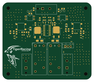
Charging
80 × 70 mm49 parts2LNo license7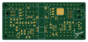 NXP
NXPRML-Yianni-Revamp
72.6 × 32.5 mm40 parts2LNo license7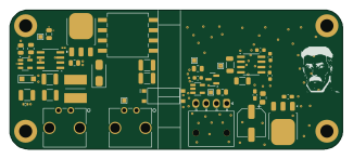 NXP
NXPRML HVI
81 × 34 mm39 parts2LNo license7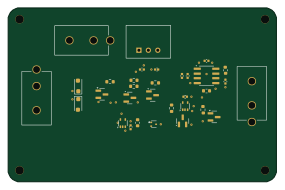
TTSI
71 × 46 mm32 parts2LNo license7
BSPD
81 × 61 mm30 parts2LNo license7
RML
85 × 50 mm25 parts4LNo license7- schematic only · 8 parts
BreathOf fresh Air
8 parts2LNo license7 
IRresistable
88 × 48 mm6 parts2LNo license7
Similar boards
 NXP
NXPMega-Cube-Board
MaltWhiskey
200 × 54 mm100 parts4LNo license763 NXP
NXP32Bit shift register
100 × 54 mm56 parts4LNo license763 NXP
NXPIC60
kiibohd
285 × 95 mm242 partsCERN-OHL-1.2415 NXP
NXPICED-R
175.4 × 145 mm163 partsCERN-OHL-1.2415 NXP
NXPTestcontroller
145.8 × 42.9 mm45 parts2LCERN-OHL-1.2415 NXP
NXPICED-L
175.4 × 145 mm163 partsCERN-OHL-1.2415