
HalfLifeProject

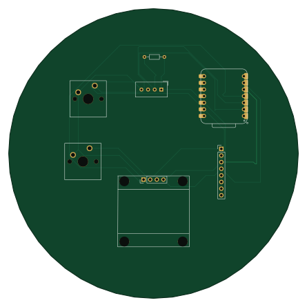
About the HalfLifeProject PCB
HalfLifeProject is an open source ESP32 PCB design by malaysianews798-png, published on GitHub. It is a 2-layer board measuring 111 × 111 mm, with 7 components from 6 distinct parts.
Its main chip is the XIAO-ESP32-C3-SMD, from the ESP32 family. Other key parts include the DHT11. By type, the board carries 2 ICs, 2 connectors, 2 switches and 1 resistor.
It belongs with the keyboards and sensors designs in this gallery.
From the project
This is a project called Starbie even though the shape doesn't look like a star... In a nutshell, This is a tamagotchi. I made this project for me to learn about PCB Design, soldering and how hardware communicate.
This is a project called Starbie even though the shape doesn't look like a star... In a nutshell, This is a tamagotchi. I made this project for me to learn about PCB Design, soldering and how hardware communicate.
How it works: how the parts fit together.
I used multiple hardware as I shown at BOM. The XIAO ESP32 C3 will be the microprocessor where it will run the code, 0.96 OLED is to show the character. MPU6050 is a sensor to detect movement, when you move the board around something will happen. DHT11 is also a sensor which detect temperature, so you could use the temperature data and…
Main components on the HalfLifeProject
HalfLifeProject bill of materials (BOM)
7 components, 6 distinct parts — part numbers from the project's BOM.
| Qty | Part | Footprint | Refs |
|---|---|---|---|
| 1 | XIAO-ESP32-C3-SMD | XIAO-ESP32-C6-DIP | U1 |
| 1 | DHT11 | Aosong_DHT11_5.5x12.0_P2.54mm | U2 |
| 1 | Conn_01x04_Pin | Display_128x64_096_I2C | J1 |
| 1 | Conn_01x08_Pin | PinHeader_1x08_P2.54mm_Vertical | J2 |
| 2 | SW_Push | SW_Cherry_MX_1.00u_PCB | SW1, SW2 |
| 1 | 10k | R_Axial_DIN0204_L3.6mm_D1.6mm_P7.62mm_Horizontal | R1 |
HalfLifeProject design files
The KiCad project lives in the malaysianews798-png/HalfLifeProject repository on GitHub; these links point at the commit this page was built from.
- Layouthalflifeproject.kicad_pcb
- Schematichalflifeproject.kicad_sch
- BOMBOM.csv
HalfLifeProject: common questions
What microcontroller does the HalfLifeProject use?
The HalfLifeProject is built around the XIAO-ESP32-C3-SMD, from the ESP32 family.
How big is the HalfLifeProject PCB?
The HalfLifeProject measures 111 × 111 mm, has 2 copper layers and is 1.6 mm thick.
How many components are on the HalfLifeProject?
7 components, from 6 distinct parts, with part numbers taken from the project's own BOM. The full bill of materials is listed on this page.
Where can I download the HalfLifeProject design files?
From the malaysianews798-png/HalfLifeProject repository on GitHub, which has the KiCad layout, the schematic and the BOM; the links under Design files point to each one.
Can I use the HalfLifeProject design in my own project?
The repository has no license, so all rights stay with malaysianews798-png. Use it as a reference, and ask the author before reusing the design.
Can I test firmware for the HalfLifeProject without the hardware?
Yes. HardLabs builds a simulation of the board from its netlist and BOM, so you can run and debug ESP32 firmware against it before you order a PCB.
Similar boards
 ESP32
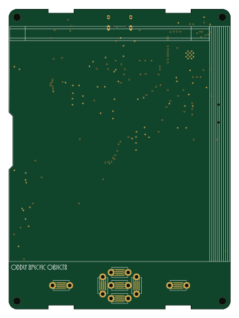
ESP32Open Book Abridged Edition
joeycastillo
85 × 115 mm65 parts2LCC-BY-SA-4.08.1k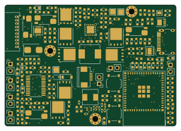 ESP32
ESP32Powertrain
byrantech
64 × 45.4 mm171 parts4LMIT4.3k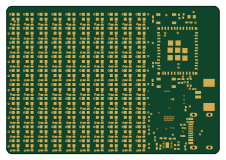 ESP32
ESP32Badge
atopile
56.3 × 39 mm239 parts4LMIT4.0k ESP32
ESP32Esp32 minimal
36.2 × 26.8 mm20 parts2LMIT4.0k ESP32
ESP32Controller
StuckAtPrototype
29 × 74 mm58 parts4LApache-2.03.8k ESP32
ESP32Racer
36 × 50.2 mm70 parts4LApache-2.03.8k