
In Board Gnia

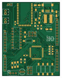
About the In Board Gnia
In Board Gnia is an open source AVR/Arduino PCB design by MbFredys, published on GitHub under the MIT license. It is a 2-layer board measuring 53 × 68 mm, with 97 components from 33 distinct parts.
Its main chip is the ATXMEGA32A4U-AU, from the AVR/Arduino family. Other key parts include the TPS61087DSCR, LM1117-3.3, L293D, FT232RL and HC-05. By type, the board carries 36 resistors, 18 capacitors, 13 diodes, 10 connectors, 6 ICs and 6 transistors.
From the project
PCB design exercises completed during a structured training course, documenting schematic capture, layout, and manufacturing outputs.
PCB design with the features of Arduino UNO but, in addition, with:
- Bluetooth module. - Motor driver. - Some push buttons, to control the motors and Bluetooth. - Several LEDs.
Main components on the In Board Gnia
In Board Gnia bill of materials (BOM)
97 components, 33 distinct parts.
| Qty | Part | Footprint | Refs |
|---|---|---|---|
| 1 | TPS61087DSCR | TPS61087 | U1 |
| 1 | LM1117-3.3 | TO-252-2 | U2 |
| 1 | L293D | DIP-16_W7.62mm | U3 |
| 1 | FT232RL | SSOP-28_5.3x10.2mm_Pitch0.65mm | U4 |
| 1 | ATXMEGA32A4U-AU | TQFP-44_10x10mm_Pitch0.8mm | U5 |
| 1 | HC-05 | HC-05 | U6 |
| 6 | MMBT3904 | SOT-23_Handsoldering | Q1, Q2, Q3, Q4, Q5, Q6 |
| 1 | Conn_01x10 | Pin_Header_Straight_1x10_Pitch2.54mm | J1 |
| 2 | Conn_01x08 | Pin_Header_Straight_1x08_Pitch2.54mm | J2, J4 |
| 1 | USB_OTG | USB_Mini-B | J3 |
| 1 | Conn_01x06 | Pin_Header_Straight_1x06_Pitch2.54mm | J5 |
| 2 | Conn_01x02 | TerminalBlock_Phoenix_MPT-2.54mm_2pol | J6, J7 |
| 2 | Conn_02x03_Odd_Even | Pin_Header_Straight_2x03_Pitch2.54mm | J8, J9 |
| 1 | Conn_01x02 | Pin_Header_Straight_1x02_Pitch2.54mm | J10 |
| 1 | R_POT_TRIM | Potentiometer_Trimmer_Bourns_PV36W | RV1 |
| 6 | SW_Push | SW_SPST_FSMSM | SW1, SW2, SW3, SW4, SW5, SW6 |
| 2 | D_Schottky | D_SMA | D1, D2 |
| 9 | LED | LED_0805_HandSoldering | D3, D4, D5, D6, D9, D10, D11, D12 +1 |
| 1 | LED_RCGB | LED_D5.0mm-4 | D7 |
| 1 | B340A-13-F | D_SMA | D8 |
Show 13 more
| Qty | Part | Footprint | Refs |
|---|---|---|---|
| 1 | 5.6uH | SDR0805 | L1 |
| 13 | 100nF | C_0805_HandSoldering | C1, C2, C5, C6, C8, C11, C12, C13 +5 |
| 2 | 10uF | CP_Elec_4x4.5 | C3, C10 |
| 1 | 1uF | C_0805_HandSoldering | C4 |
| 1 | 22uF | CP_Elec_4x5.3 | C7 |
| 1 | 820pF | C_0805_HandSoldering | C9 |
| 13 | 10K | R_1206_HandSoldering | R1, R2, R11, R12, R19, R20, R23, R24 +5 |
| 11 | 330 | R_1206_HandSoldering | R3, R4, R5, R6, R7, R8, R9, R15 +3 |
| 1 | 232K | R_1206_HandSoldering | R10 |
| 1 | 105K | R_1206_HandSoldering | R13 |
| 1 | 26.7K | R_1206_HandSoldering | R14 |
| 8 | 1K | R_1206_HandSoldering | R17, R18, R21, R22, R29, R30, R33, R34 |
| 1 | 2K | R_1206_HandSoldering | R36 |
In Board Gnia design files
The KiCad project lives in the MbFredys/PCB-designs-for-PLATZI-course repository on GitHub; these links point at the commit this page was built from.
In Board Gnia: common questions
What microcontroller does the In Board Gnia use?
The In Board Gnia is built around the ATXMEGA32A4U-AU, from the AVR/Arduino family.
How big is the In Board Gnia?
The In Board Gnia measures 53 × 68 mm, has 2 copper layers and is 1.6 mm thick.
How many components are on the In Board Gnia?
97 components, from 33 distinct parts. The full bill of materials is listed on this page.
Where can I download the In Board Gnia design files?
From the MbFredys/PCB-designs-for-PLATZI-course repository on GitHub, which has the KiCad layout; the links under Design files point to each one.
Can I use the In Board Gnia design in my own project?
Yes, under the terms of its MIT license, which MbFredys chose for the repository.
Can I test firmware for the In Board Gnia without the hardware?
Yes. HardLabs builds a simulation of the board from its netlist and BOM, so you can run and debug AVR/Arduino firmware against it before you order a PCB.
More boards in PCB-designs-for-PLATZI-course
Similar boards
 AVR/Arduino
Redox keyboard
mattdibi
162.2 × 126.5 mm77 parts2LMIT2.0k AVR/Arduino
ModuleV450
stuartpittaway
30 × 61.4 mm39 parts2LCC-BY-NC-4.01.1k AVR/Arduino
V4
30 × 50 mm38 parts2LCC-BY-NC-4.01.1k AVR/Arduino
Discipline
coseyfannitutti
304.9 × 122.8 mm170 parts2LCC-BY-NC-4.01.0k AVR/Arduino
Megadesk
gcormier
41.7 × 32.2 mm23 parts2LGPL-3.0818 AVR/Arduino
Easyduino Atmega Nano
Hanqaqa
43.4 × 18 mm30 parts4LCERN-OHL-P-2.0746