
USB-C Receptacle Tester

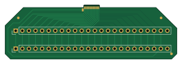
About the USB-C Receptacle Tester PCB
USB-C Receptacle Tester is an open source PCB design by monero-project, published on GitHub under the CERN-OHL-1.2 license. It is a 2-layer board measuring 66 × 21 mm, with 3 components from 2 distinct parts.
From the project
The Sekura Monero Hardware Wallet
Example text to help understand contents and subdirectories.
USB-C Receptacle Tester bill of materials (BOM)
3 components, 2 distinct parts — part numbers from the project's BOM.
| Qty | Part | Footprint | Refs |
|---|---|---|---|
| 2 | CONN_01X24 | Pin_Header_Straight_1x24_Pitch2.54mm | J1, J3 |
| 1 | USB_C_Plug | USB_C_Plug_Molex_105444 | P1 |
USB-C Receptacle Tester design files
The KiCad project lives in the monero-project/kastelo repository on GitHub; these links point at the commit this page was built from.
USB-C Receptacle Tester: common questions
How big is the USB-C Receptacle Tester PCB?
The USB-C Receptacle Tester measures 66 × 21 mm, has 2 copper layers and is 1.6 mm thick.
How many components are on the USB-C Receptacle Tester?
3 components, from 2 distinct parts, with part numbers taken from the project's own BOM. The full bill of materials is listed on this page.
Where can I download the USB-C Receptacle Tester design files?
From the monero-project/kastelo repository on GitHub, which has the KiCad layout and the BOM; the links under Design files point to each one.
Can I use the USB-C Receptacle Tester design in my own project?
Yes, under the terms of its CERN-OHL-1.2 license, which monero-project chose for the repository.
More boards in kastelo
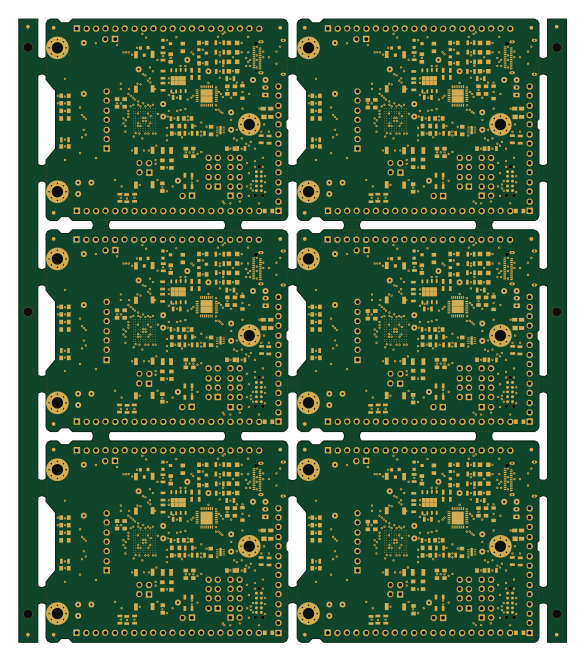
Breakpanel
145 × 165 mm105 parts2LCERN-OHL-1.2115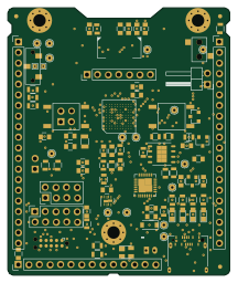
Breakneck
53.3 × 64 mm89 parts2LCERN-OHL-1.2115
AStable Timer LED Badge
100 × 95 mm78 parts2LCERN-OHL-1.2115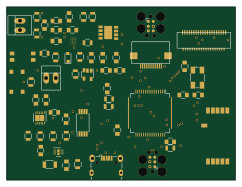 STM32
Ledgblue
60.5 × 45.8 mm59 parts2LCERN-OHL-1.2115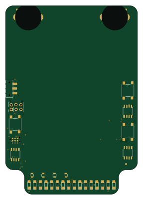 AVR/Arduino
DefcoNFC Hardware Badge
70 × 100 mm31 parts2LCERN-OHL-1.2115
HCPP NFC Hardware Badge
80 × 71 mm5 parts2LCERN-OHL-1.2115