
Generic Scan Selector

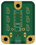
About the Generic Scan Selector PCB
Generic Scan Selector is an open source PCB design by nanographs, published on GitHub. It is a 2-layer board measuring 30 × 38 mm, with 9 components from 9 distinct parts.
By type, the board carries 7 connectors and 1 diode.
From the project
Just what you need to control the beam and get an image.
Just what you need to control the beam and get an image.
Glasgow makes getting bytes in and out of the FPGA over USB radically more accessible. We use that to make getting data into and out of your microscope radically more accessible.
- [X] Order and test rev 1 PCBs (Design not uploaded, required significant rework) - [X] Capture 16,384 x 16,384 images - [X] Live viewer fast enough to focus and stigmate with - [X] Raster pattern mode at 16,384 x 16,384 image resolution, with 8-bit grayscale dwell times - [X] Order and test V1.0 PCBs - [x] Refactor gateware to support 16-bit grayscale…
Generic Scan Selector bill of materials (BOM)
9 components, 9 distinct parts — part numbers from the project's BOM.
| Qty | Part | Footprint | Refs |
|---|---|---|---|
| 1 | X_Internal | PinHeader_1x02_P2.54mm_Vertical | J1 |
| 1 | Y_Internal | PinHeader_1x02_P2.54mm_Vertical | J2 |
| 1 | X_Out | PinHeader_1x02_P2.54mm_Vertical | J3 |
| 1 | Y_Out | PinHeader_1x02_P2.54mm_Vertical | J4 |
| 1 | X_External | PinHeader_1x02_P2.54mm_Vertical | J5 |
| 1 | Y_External | PinHeader_1x02_P2.54mm_Vertical | J6 |
| 1 | M8_CONN_01X03_PIN_SHIELDED M8_conn_01x03_Pin_Shielded | M8_conn_01x03_Pin_Shielded_Right_Angle | J7 |
| 1 | Omron G6K-2P-RF | Omron G6K-2P-RF DPDT Relay | RY1 |
| 1 | 1N4007 | D_DO-41_SOD81_P10.16mm_Horizontal | D1 |
Generic Scan Selector design files
The KiCad project lives in the nanographs/Open-Beam-Interface repository on GitHub; these links point at the commit this page was built from.
- LayoutHardware/PCBs/Interface selectors and drivers/Generic Scan Selector/Generic Scan Selector.kicad_pcb
- SchematicHardware/PCBs/Interface selectors and drivers/Generic Scan Selector/Generic Scan Selector.kicad_sch
- BOMHardware/PCBs/Interface selectors and drivers/Generic Scan Selector/Generic Scan Selector-bom.csv
Generic Scan Selector: common questions
How big is the Generic Scan Selector PCB?
The Generic Scan Selector measures 30 × 38 mm, has 2 copper layers and is 1.6 mm thick.
How many components are on the Generic Scan Selector?
9 components, from 9 distinct parts, with part numbers taken from the project's own BOM. The full bill of materials is listed on this page.
Where can I download the Generic Scan Selector design files?
From the nanographs/Open-Beam-Interface repository on GitHub, which has the KiCad layout, the schematic and the BOM; the links under Design files point to each one.
Can I use the Generic Scan Selector design in my own project?
The repository has no license, so all rights stay with nanographs. Use it as a reference, and ask the author before reusing the design.
More boards in Open-Beam-Interface
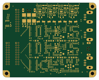
Open Beam Interface
100 × 80 mm282 parts4LNo license371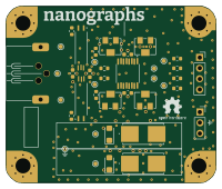
Beam Offset Switch
50 × 42 mm29 parts4LNo license371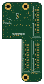
OBI Data Interconnect
40.3 × 80 mm19 parts4LNo license371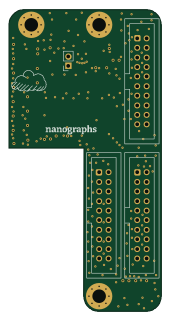
Data Interconnect revA2
40.3 × 80 mm19 parts4LNo license371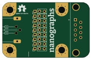
DB9 High-Low Signal Generator
47 × 30 mm10 parts2LNo license371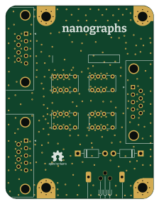
DB9 Differential Signal Selector
55 × 72 mm7 parts4LNo license371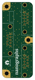
DSC DB9 Splitter
28 × 70 mm6 parts4LNo license371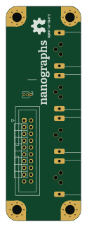
Digital IO Breakout
28 × 80 mm6 parts2LNo license371
DSC Scan Selector
64 × 46.5 mm5 parts4LNo license371