
POWER

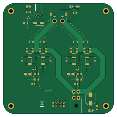
About the POWER PCB
POWER is an open source PCB design by Oerdna, published on GitHub under the AGPL-3.0 license. It is a 4-layer board measuring 100 × 100 mm, with 39 components from 18 distinct parts.
Other key parts include the IR2104. By type, the board carries 15 diodes, 8 resistors, 5 transistors, 5 capacitors, 4 connectors and 2 ICs.
It belongs with the test & measurement designs in this gallery.
From the project
Redesigned PCB for simultaneous Peltier control and surface resistance measurement
More details about the device can be understood from the schematic drawing here. The notes are in Russian.
The controller for the complex is STM32L432KC Nucleo.
In this case are studing the I - V characteristic of an element depending on the temperature of the sample. It is important to understand the I – V characteristic near the metal-insulator phase transition (MIT), which is about 68 degrees Celsius. You must understand that the ultimate goal is to stabilize the temperature to a specific value. More about the TEC control [2]
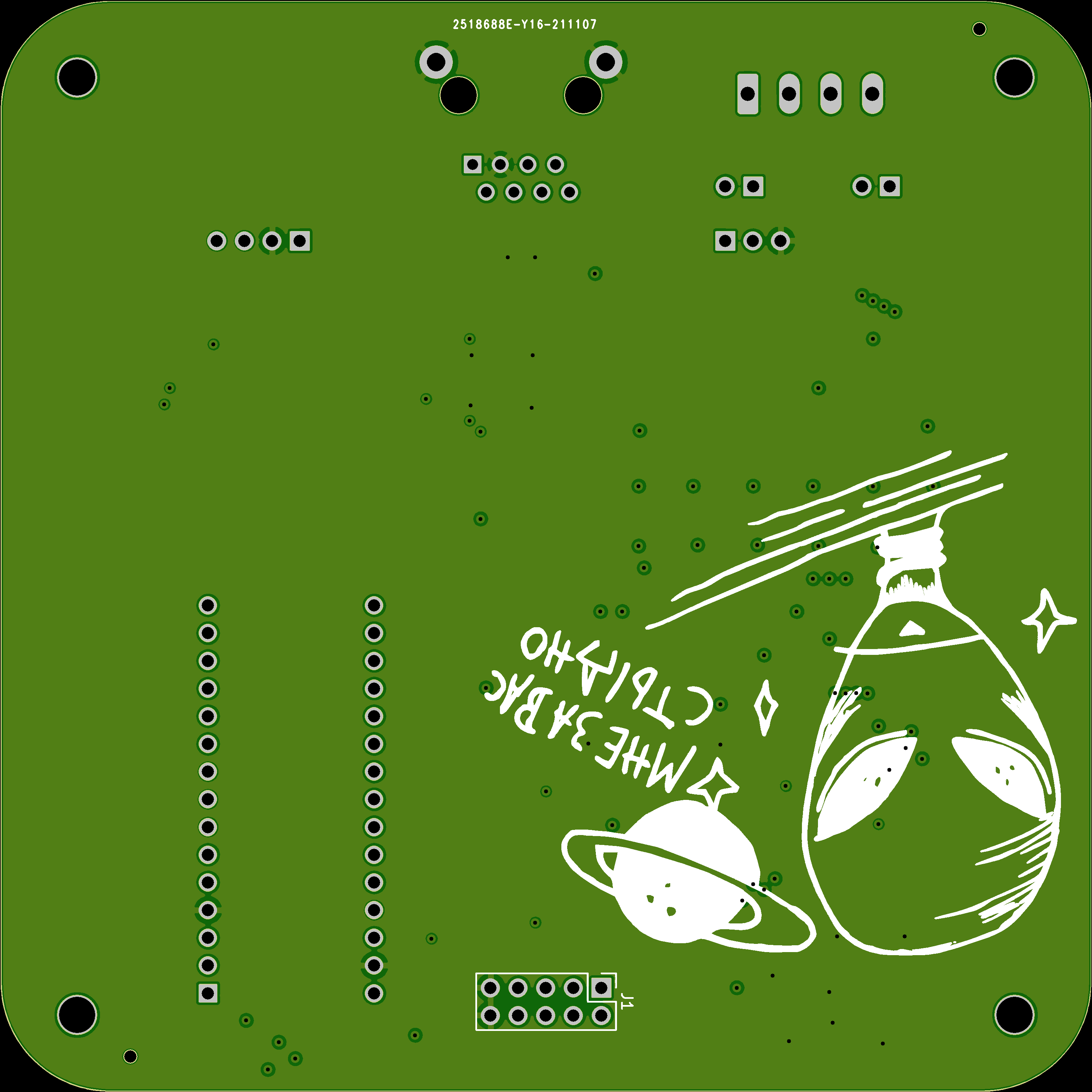
Main components on the POWER
POWER bill of materials (BOM)
39 components, 18 distinct parts.
| Qty | Part | Footprint | Refs |
|---|---|---|---|
| 2 | IR2104 | SOIC-8_3.9x4.9mm_P1.27mm | U3, U4 |
| 4 | IRF7403 | SOIC-8_3.9x4.9mm_P1.27mm | Q1, Q2, Q4, Q5 |
| 1 | FDV303N | SOT-23 | Q3 |
| 1 | J_PCB_DOWN | PinHeader_2x05_P2.54mm_Vertical | J2 |
| 1 | IN_12V_POWER | Molex_Mini-Fit_Jr_5569-04A2_2x02_P4.20mm_Horizontal | J4 |
| 1 | J_COOLER | PinHeader_1x03_P2.54mm_Horizontal | J5 |
| 1 | J_TERMO | Amass_XT60PW-M | J6 |
| 2 | US2MA | D_SMA | D2, D12 |
| 1 | 12V_LED | LED_1206_3216Metric_Castellated | D3 |
| 8 | 1N4148W | D_SOD-123 | D4, D5, D6, D7, D13, D14, D15, D16 |
| 1 | FUN_LED | LED_1206_3216Metric_Castellated | D8 |
| 1 | 1N4001 | D_SMA-SMB_Universal_Handsoldering | D9 |
| 2 | LED | LED_0805_2012Metric_Castellated | D10, D11 |
| 2 | 10uF | C_0805_2012Metric_Pad1.18x1.45mm_HandSolder | C10, C13 |
| 2 | 1uF | C_0805_2012Metric_Pad1.18x1.45mm_HandSolder | C11, C14 |
| 1 | 220uF | CP_Elec_8x10.5 | C12 |
| 4 | 1k | R_1206_3216Metric_Pad1.30x1.75mm_HandSolder | R10, R13, R14, R15 |
| 4 | 47 | R_2512_6332Metric_Pad1.40x3.35mm_HandSolder | R11, R12, R16, R17 |
POWER design files
The KiCad project lives in the Oerdna/V2_TEC repository on GitHub; these links point at the commit this page was built from.
- LayoutTEC2/POWER.kicad_pcb
POWER: common questions
How big is the POWER PCB?
The POWER measures 100 × 100 mm, has 4 copper layers and is 1.6 mm thick.
How many components are on the POWER?
39 components, from 18 distinct parts. The full bill of materials is listed on this page.
Where can I download the POWER design files?
From the Oerdna/V2_TEC repository on GitHub, which has the KiCad layout; the links under Design files point to each one.
Can I use the POWER design in my own project?
Yes, under the terms of its AGPL-3.0 license, which Oerdna chose for the repository.
More boards in V2_TEC
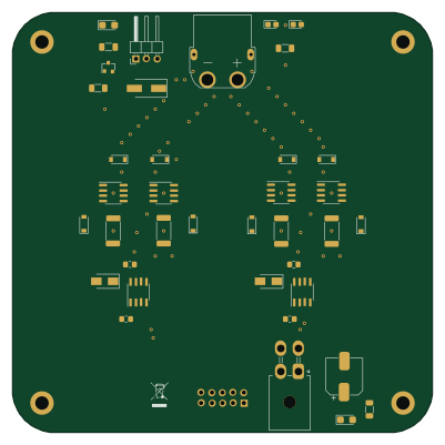
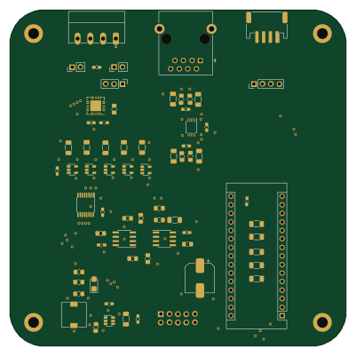
Similar boards
LevelShifter
gusmanb
28.3 × 39.8 mm21 parts2LGPL-3.05.0k
StackLink
52.3 × 10.5 mm5 parts2LGPL-3.05.0k
AnalyzerBoxPCB fork
52.7 × 47.9 mm54 parts4LGPL-3.05.0k
EleLab v2 Bus100
Chrismettal
100 × 100 mm37 parts2LGPL-3.0528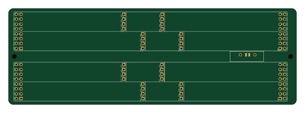
EleLab v2 Bus150
150 × 50 mm37 parts2LGPL-3.0528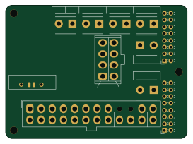
EleLab v2 PowerFeed
68 × 50 mm11 parts2LGPL-3.0528