
Pergola

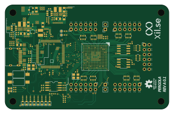
About the Pergola PCB
Pergola is an open source FPGA PCB design by pergola-fpga, published on GitHub under the MIT license. It is a 4-layer board measuring 85 × 54 mm, with 136 components from 39 distinct parts.
Its main chip is the LFE5U-12F-6BG256C, from the FPGA family. Other key parts include the SY8120B1ABC, XC6206P25, SPI Flash W25Q128JVSIQ, MIMXRT1011DAE5A and MAX803SQ308T1G. By type, the board carries 47 resistors, 44 capacitors, 10 ICs, 9 jumpers, 9 diodes and 5 connectors.
It belongs with the dev boards & breakouts designs in this gallery.
From the project
Low-cost ECP5 FPGA development board
The Pergola FPGA board is a low-cost, open-source FPGA development board featuring the Lattice ECP5 FPGA.
A handful of units have been built for initial test and bringup populated with LFE5U-12F-8BG256C.
It has been tested and works if the fixes below are applied.
- iMX ROM bootloader freezes because the UART RX pin is pulled low by the FPGA during boot. (FPGA pin is PL35BVREF16) A 4K7 pull-up is probably not enough, the voltage drops to 2.9V. Workaround: Bodge a 1K pull-up between UARTRX and 3V3. - Wrong load caps for the xtal. Should be 20pF. - SWD IO and CLK are swapped on the silk. -…
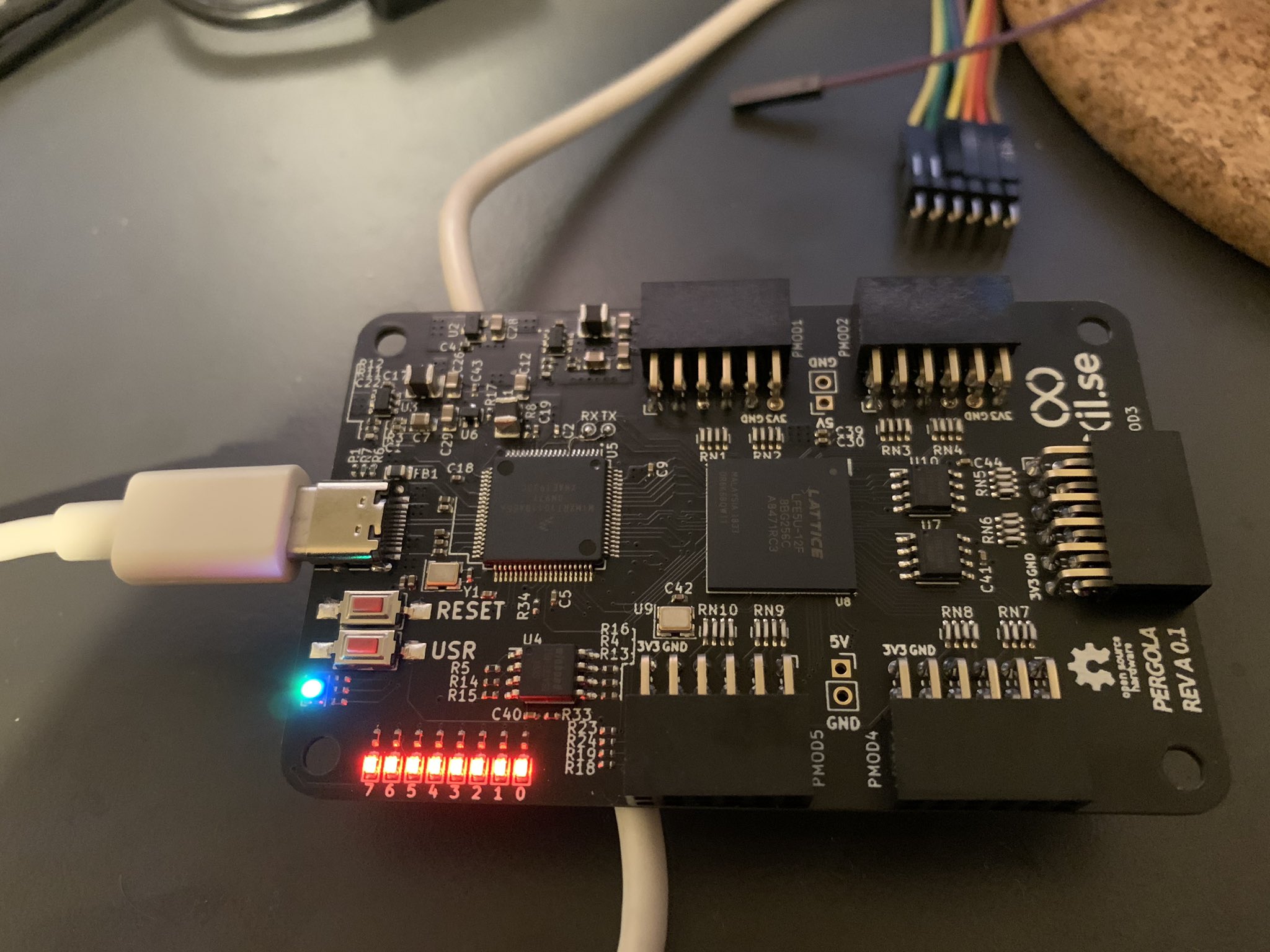
Main components on the Pergola
Pergola bill of materials (BOM)
136 components, 39 distinct parts — part numbers from the project's BOM.
| Qty | Part | Footprint | Refs |
|---|---|---|---|
| 2 | SY8120B1ABC | SOT-23-6 | U1, U3 |
| 1 | XC6206P25 | SOT-23 | U2 |
| 1 | SPI Flash W25Q128JVSIQ | SOA008-150-208mil | U4 |
| 1 | MIMXRT1011DAE5A | LQFP-80_12x12mm_P0.5mm | U5 |
| 1 | MAX803SQ308T1G | SOT-323_SC-70 | U6 |
| 2 | SPI RAM LY68L6400SLIT | SOIC-8_3.9x4.9mm_P1.27mm | U7, U10 |
| 1 | LFE5U-12F-6BG256C | cabga256 | U8 |
| 1 | 16MHz 20ppm | Crystal_SMD_3225-4Pin_3.2x2.5mm | U9 |
| 1 | 24MHz 10ppm | Crystal_SMD_3225-4Pin_3.2x2.5mm | Y1 |
| 1 | USB_C_RECEPTACLE_USB2.0 USB_C_Receptacle_USB2.0 | USB_C_Receptacle_GT-USB-7010 | J1 |
| 1 | DNP Conn_02x02_Odd_Even | PinHeader_2x02_P2.54mm_Vertical_SMD | J2 |
| 2 | DNP Conn_01x02 | PinSocket_1x02_P2.54mm_Vertical | J3, J5 |
| 1 | DNP Conn_02x03_Odd_Even | PinHeader_2x03_P2.54mm_Vertical_SMD | J4 |
| 9 | 4K7 | JP_3_0402_1005Metric | JP1, JP2, JP3, JP4, JP5, JP6, JP7, JP8 +1 |
| 5 | CONN_02X06_TOP_BOTTOM Conn_02x06_Top_Bottom | PMOD_Socket_2x06_P2.54mm_Horizontal | PMOD1, PMOD2, PMOD3, PMOD4, PMOD5 |
| 2 | SW_Push | SW_SPST_FSMSM | SW1, SW2 |
| 1 | LED_ARGB | LED_Cree-PLCC4_2x2mm_CW | D1 |
| 8 | LED | LED_0603_1608Metric | D2, D3, D4, D5, D6, D7, D8, D9 |
| 1 | Ferrite_Bead | L_0805_2012Metric | FB1 |
| 3 | 4u7 1A | L_1008_1210 | L1, L2, L3 |
Show 19 more
| Qty | Part | Footprint | Refs |
|---|---|---|---|
| 21 | 100N 100n | C_0402_1005Metric | C1, C3, C16, C17, C20, C23, C30, C31 +13 |
| 7 | 220N 220n | C_0402_1005Metric | C2, C5, C8, C9, C13, C18, C19 |
| 3 | 4U7 4u7 | C_0402_1005Metric | C4, C10, C15 |
| 8 | 22U 22u | C_0805_2012Metric | C6, C7, C12, C25, C26, C27, C28, C29 |
| 2 | 4P7 20p | C_0402_1005Metric | C11, C14 |
| 2 | 22P 22p | C_0402_1005Metric | C21, C22 |
| 1 | 10U 10u | C_0402_1005Metric | C24 |
| 1 | 100K | R_0402_1005Metric | R1 |
| 7 | 10K | R_0402_1005Metric | R2, R3, R13, R14, R15, R16, R17 |
| 3 | 1K | R_0402_1005Metric | R4, R36, R37 |
| 7 | 4K7 | R_0402_1005Metric | R5, R18, R19, R23, R24, R33, R34 |
| 2 | 5K1 | R_0402_1005Metric | R6, R7 |
| 1 | 30K | R_0402_1005Metric | R8 |
| 2 | 15K | R_0402_1005Metric | R9, R11 |
| 1 | 18K | R_0402_1005Metric | R10 |
| 1 | 3K3 | R_0402_1005Metric | R12 |
| 11 | 4K7 10K | R_0402_1005Metric | R20, R21, R22, R25, R26, R27, R28, R29 +3 |
| 1 | DNP | R_0402_1005Metric | R35 |
| 10 | 22R_X4 22R_x4 | R_Array_Convex_4x0603 | RN1, RN2, RN3, RN4, RN5, RN6, RN7, RN8 +2 |
Pergola design files
The KiCad project lives in the pergola-fpga/pergola repository on GitHub; these links point at the commit this page was built from.
Pergola: common questions
What microcontroller does the Pergola use?
The Pergola is built around the LFE5U-12F-6BG256C, from the FPGA family.
How big is the Pergola PCB?
The Pergola measures 85 × 54 mm, has 4 copper layers and is 1.2 mm thick.
How many components are on the Pergola?
136 components, from 39 distinct parts, with part numbers taken from the project's own BOM. The full bill of materials is listed on this page.
Where can I download the Pergola design files?
From the pergola-fpga/pergola repository on GitHub, which has the KiCad layout and the BOM; the links under Design files point to each one.
Can I use the Pergola design in my own project?
Yes, under the terms of its MIT license, which pergola-fpga chose for the repository.
Can I test firmware for the Pergola without the hardware?
Yes. HardLabs builds a simulation of the board from its netlist and BOM, so you can run and debug FPGA firmware against it before you order a PCB.
Similar boards
 FPGA
FPGABase board
GlasgowEmbedded
80 × 49 mm222 parts4L0BSD2.2k FPGA
FPGAThunderscope Rev5.3
EEVengers
122.5 × 103.5 mm817 parts6LMIT1.3k FPGA
FPGAUsb sniffer
ataradov
58.2 × 38.1 mm86 parts2LBSD-3-Clause1.3k FPGA
FPGAIcepi zero
cheyao
65 × 30 mm143 parts4LSHL-2.1828 FPGA
FPGARadioberry
pa3gsb
65 × 56 mm143 parts4LNo license675 FPGA
FPGAHaasoscopePro
drandyhaas
224.5 × 160 mm586 parts10LMIT471