
EKO MyMiner

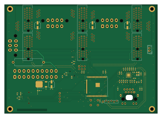
About the EKO MyMiner PCB
EKO MyMiner is an open source ESP32 PCB design by phil31, published on GitHub under the GPL-3.0 license. It is a 4-layer board measuring 140 × 100 mm, with 66 components from 42 distinct parts.
Its main chip is the 25MHZ, from the ESP32 family. Other key parts include the SN74AXC4T245BQB and MCP1824T-3302E/OT. By type, the board carries 25 resistors, 16 capacitors, 15 connectors, 3 ICs, 3 transistors and 1 crystal.
From the project
rackable miner
Power board : - designed with TPS53667 / 5 Phases / 0.5 to 2.5V, up to 300Watts
AsicBoards : - 16 x BM1366 : 8 TH/s - Efficiency 25J/TH - 16 x BM1368 : 9.5 TH/s - Efficiency 18J/TH - 10 x BM1370 : 10 TH/s - Efficiency 15J/TH

Main components on the EKO MyMiner
EKO MyMiner bill of materials (BOM)
66 components, 42 distinct parts — part numbers from the project's BOM.
| Qty | Part | Footprint | Refs |
|---|---|---|---|
| 1 | SN74AXC4T245BQB LAN8720A | LAN8720_VQFN-24-1EP_4x4mm_P0.5mm_EP2.5x2.5mm_ThermalVias | U1 |
| 1 | 25MHZ ESP32-WROOM-32U | ESP32-WROOM-32U | U2 |
| 1 | MCP1824T-3302E/OT NCP1117-3.3_TO252 | TO-252-2 | U3 |
| 1 | BSS138 | SOT-23 | Q1 |
| 2 | BSS138 | SOT-23 | Q2, Q3 |
| 1 | ASE-xxxMHz | Oscillator_SMD_Abracon_ASE-4Pin_3.2x2.5mm | X1 |
| 2 | 10018784-10210TLF | AMPHENOL_10018784-10210TLF | J1, J2 |
| 1 | CONN_01X04 10018784-10210TLF | AMPHENOL_10018784-10210TLF | J3 |
| 1 | CONN_01X04 RJ45_LMJ2138814S0L1T1C | LMJ2138814SOL1T1C | J4 |
| 1 | Conn_01x02_Pin | JST_EH_B2B-EH-A_1x02_P2.50mm_Vertical | J5 |
| 1 | Conn_01x06_Pin | EKO_ESP_ISP | J6 |
| 1 | Conn_02x10_Top_Bottom | Molex_Mini-Fit_Jr_5566-20A_2x10_P4.20mm_Vertical | J7 |
| 1 | Conn_02x03_Odd_Even | PinHeader_2x03_P2.54mm_Vertical | J8 |
| 1 | Conn_01x12_Pin | LCD LBS147TC-IG01 | J9 |
| 2 | 5566-08A | Molex_Mini-Fit_Jr_5566-08A2_2x04_P4.20mm_Vertical | J10, J11 |
| 1 | Conn_02x03_Counter_Clockwise | Molex_Mini-Fit_Jr_5566-06A2_2x03_P4.20mm_Vertical | J12 |
| 3 | 10018784-10210TLF | AMPHENOL_10018784-10210TLF | J15, J16, J17 |
| 1 | SW_SPST | SW_PUSH_6mm_H9.5mm | SW1 |
| 1 | WS2812B-2020 | WS2812B2020 | D1 |
| 1 | 150NH L | L_0805_2012Metric | L1 |
Show 22 more
| Qty | Part | Footprint | Refs |
|---|---|---|---|
| 1 | 100NF 100uF | CP_Elec_5x5.7 | C1 |
| 3 | 100NF 100nF | C_0603_1608Metric | C2, C4, C6 |
| 5 | 1UF 100nF | C_0603_1608Metric | C3, C5, C9, C10, C11 |
| 1 | 100NF 1µF | C_0603_1608Metric | C7 |
| 1 | 1UF 470pF | C_0603_1608Metric | C8 |
| 1 | 22nF | C_0603_1608Metric | C12 |
| 2 | 100uF | CP_Elec_5x5.7 | C13, C15 |
| 1 | 100nF | C_0603_1608Metric | C14 |
| 1 | 1UF 100uF | CP_Elec_5x5.7 | C16 |
| 1 | 180R 0R | R_0603_1608Metric | R1 |
| 2 | 10K | R_0603_1608Metric | R2, R3 |
| 1 | 10K 1K5 | R_0603_1608Metric | R4 |
| 2 | 10K 33R | R_0603_1608Metric | R5, R7 |
| 1 | 180R 33R | R_0603_1608Metric | R6 |
| 3 | 10R | R_0603_1608Metric | R8, R9, R10 |
| 4 | 49R9 | R_0603_1608Metric | R11, R12, R14, R15 |
| 1 | 12K1 1% | R_0603_1608Metric | R13 |
| 2 | 220R | R_0603_1608Metric | R16, R17 |
| 5 | 10K | R_0603_1608Metric | R18, R19, R20, R22, R23 |
| 1 | 20R | R_0603_1608Metric | R21 |
| 1 | 50R | R_Axial_Power_L25.0mm_W6.4mm_P27.94mm | R24 |
| 1 | 10K | R_0402_1005Metric | R25 |
EKO MyMiner design files
The KiCad project lives in the phil31/BOX-Miner repository on GitHub; these links point at the commit this page was built from.
EKO MyMiner: common questions
What microcontroller does the EKO MyMiner use?
The EKO MyMiner is built around the 25MHZ, from the ESP32 family.
How big is the EKO MyMiner PCB?
The EKO MyMiner measures 140 × 100 mm, has 4 copper layers and is 1.6 mm thick.
How many components are on the EKO MyMiner?
66 components, from 42 distinct parts, with part numbers taken from the project's own BOM. The full bill of materials is listed on this page.
Where can I download the EKO MyMiner design files?
From the phil31/BOX-Miner repository on GitHub, which has the KiCad layout, the schematic and the BOM; the links under Design files point to each one.
Can I use the EKO MyMiner design in my own project?
Yes, under the terms of its GPL-3.0 license, which phil31 chose for the repository.
Can I test firmware for the EKO MyMiner without the hardware?
Yes. HardLabs builds a simulation of the board from its netlist and BOM, so you can run and debug ESP32 firmware against it before you order a PCB.
More boards in BOX-Miner
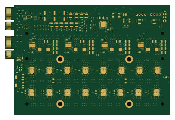
EKO Miner BM1366-13xx 16-01A
148.4 × 99.8 mm532 parts6LGPL-3.05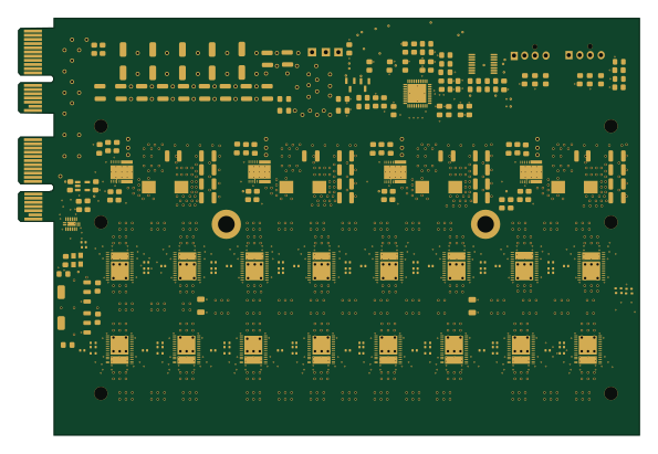
EKO Miner BM1366-13xx 16-01B
148.4 × 99.8 mm514 parts6LGPL-3.05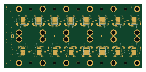
AsicsBoard - 16xBM1368 - 01A
139.8 × 65 mm394 parts6LGPL-3.05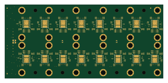
AsicsBoard - 16xBM1366 - 01A
140 × 65 mm368 parts6LGPL-3.05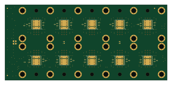
AsicsBoard - 10xBM1370 - 01A
139.8 × 65 mm256 parts6LGPL-3.05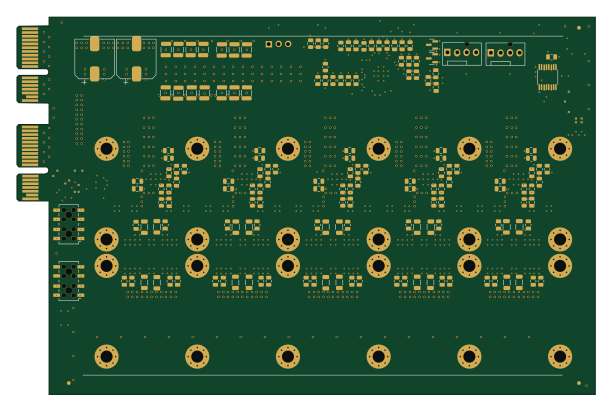
EKO Miner PowerBoard-53667
153 × 99.8 mm240 parts6LGPL-3.05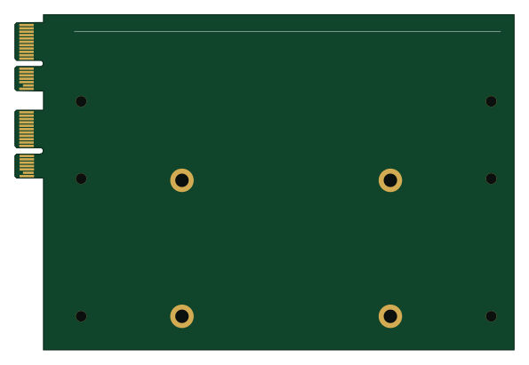
EKO Miner BM1366-13xx 16-01A PCBonly
148.4 × 99.8 mm38 parts6LGPL-3.05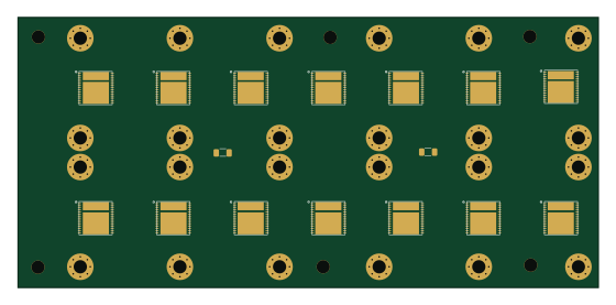
EKO Miner AsicsBoard Template 01A
139.8 × 65 mm14 parts6LGPL-3.05
Similar boards
 ESP32
OSO-BOOK-B1
joeycastillo
85 × 115 mm65 parts2LCC-BY-SA-4.08.1k ESP32
Powertrain
byrantech
64 × 45.4 mm171 parts4LMIT4.3k ESP32
Badge
atopile
56.3 × 39 mm239 parts4LMIT4.0k ESP32
Esp32 minimal
36.2 × 26.8 mm20 parts2LMIT4.0k ESP32
Controller
StuckAtPrototype
29 × 74 mm58 parts4LApache-2.03.8k ESP32
Racer
36 × 50.2 mm70 parts4LApache-2.03.8k