
Mainboard layout V1

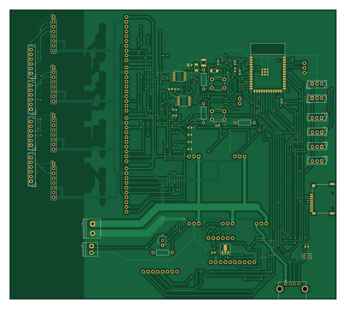
About the Mainboard layout V1 PCB
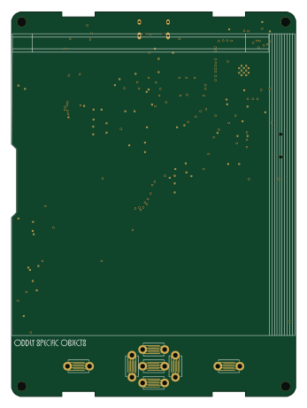
Mainboard layout V1 is an open source ESP32 PCB design by ReadHeadRedemption, published on GitHub. It is a 2-layer board measuring 172 × 152.9 mm, with 64 components from 28 distinct parts.
Its main chip is the ESP32-S3-WROOM-1, from the ESP32 family. Other key parts include the PCA9534PW. By type, the board carries 32 connectors, 19 resistors, 5 capacitors, 3 ICs, 2 transistors and 2 switches.
From the project
The master schematic is within "Senior design mainboard32826 backup"
The master schematic is within "Senior design mainboard32826 backup"
This was the version that everything was verified in as of 4/10/2026
Then for the sake of layout, and neatness broken out into their own project files for each discrete board. This includes swapping and non-swapping
Mainbourd layout pre-weeks check 1 has most up to date version of mainboard PCB this will eventually be made neater again as development continues but this is noted to avoid mistakes for now
Main components on the Mainboard layout V1
Mainboard layout V1 bill of materials (BOM)
64 components, 28 distinct parts — part numbers from the project's BOM.
| Qty | Part | Footprint | Refs |
|---|---|---|---|
| 2 | PCA9534PW | TSSOP-16_4.4x5mm_P0.65mm | U3, U5 |
| 1 | ESP32-S3-WROOM-1 | ESP32-S3-WROOM-1 | U12 |
| 1 | 2DD1664 | SOT-89-3 | Q2 |
| 1 | 2N7000 | TO-92_Inline_Wide_SGD | Q5 |
| 1 | MSD-1-A | CONN9_MSD-1_CUD | J1 |
| 1 | Screw_Terminal_2_P5.00mm | TerminalBlock_Phoenix_PT-1,5-2-5.0-H_1x02_P5.00mm_Horizontal | J2 |
| 1 | Screw_Terminal_2_P3.50mm | TerminalBlock_Phoenix_PT-1,5-2-3.5-H_1x02_P3.50mm_Horizontal | J3 |
| 4 | JST_06 | JST_EH_B6B-EH-A_1x06_P2.50mm_Vertical | J4, J6, J7, J12 |
| 1 | Conn_01x06 | 1x06_P2.54mm | J8 |
| 5 | Conn_01x10 | 1x10_P2.54mm | J9, J18, J20, J23, J24 |
| 1 | Conn_01x02 | 1x02_P2.54mm | J10 |
| 6 | Conn_01x03 | 1x03_P2.54mm | J11, J14, J15, J22, J28, J29 |
| 1 | Conn_01x08 | 1x08_P2.54mm | J13 |
| 4 | PINHD_1x8_Male | PinHeader_1x08_P2.54mm_Vertical | J16, J17, J19, J21 |
| 1 | USB-A1VSB6 | USB_A_Kycon_KUSBX-AS1N-B_Horizontal | J30 |
| 6 | JST_03 | JST_EH_B3B-EH-A_1x03_P2.50mm_Vertical | J31, J34, J35, J36, J37, J38 |
| 2 | Push_Button | SW_PUSH_6mm | SW8, SW9 |
| 1 | LED | LED_0603_1608Metric | D9 |
| 1 | 1nF_Ceramic | C_Disc_D5.0mm_W2.5mm_P2.50mm | C1 |
| 1 | 10uF | C_1210_3225Metric | C2 |
Show 8 more
| Qty | Part | Footprint | Refs |
|---|---|---|---|
| 3 | 0.1uF | C_0603_1608Metric | C3, C16, C23 |
| 1 | 1k | R_Axial_DIN0207_L6.3mm_D2.5mm_P10.16mm_Horizontal | R1 |
| 2 | 10k | R_Axial_DIN0207_L6.3mm_D2.5mm_P10.16mm_Horizontal | R5, R39 |
| 1 | 1M | R_0603_1608Metric | R6 |
| 2 | 1k | R_1206_3216Metric_Pad1.30x1.75mm_HandSolder | R36, R37 |
| 1 | 100k | R_Axial_DIN0207_L6.3mm_D2.5mm_P10.16mm_Horizontal | R40 |
| 8 | 10k | R_0603_1608Metric | R48, R49, R50, R52, R53, R54, R55, R56 |
| 4 | RK73H1ETTP4701F 4K7 | R_0603_1608Metric | R89, R90, R91, R107 |
Mainboard layout V1 design files
The KiCad project lives in the ReadHeadRedemption/SeniorDesignSp26Su26 repository on GitHub; these links point at the commit this page was built from.
Mainboard layout V1: common questions
What microcontroller does the Mainboard layout V1 use?
The Mainboard layout V1 is built around the ESP32-S3-WROOM-1, from the ESP32 family.
How big is the Mainboard layout V1 PCB?
The Mainboard layout V1 measures 172 × 152.9 mm, has 2 copper layers and is 1.6 mm thick.
How many components are on the Mainboard layout V1?
64 components, from 28 distinct parts, with part numbers taken from the project's own BOM. The full bill of materials is listed on this page.
Where can I download the Mainboard layout V1 design files?
From the ReadHeadRedemption/SeniorDesignSp26Su26 repository on GitHub, which has the KiCad layout and the BOM; the links under Design files point to each one.
Can I use the Mainboard layout V1 design in my own project?
The repository has no license, so all rights stay with ReadHeadRedemption. Use it as a reference, and ask the author before reusing the design.
Can I test firmware for the Mainboard layout V1 without the hardware?
Yes. HardLabs builds a simulation of the board from its netlist and BOM, so you can run and debug ESP32 firmware against it before you order a PCB.
More boards in SeniorDesignSp26Su26
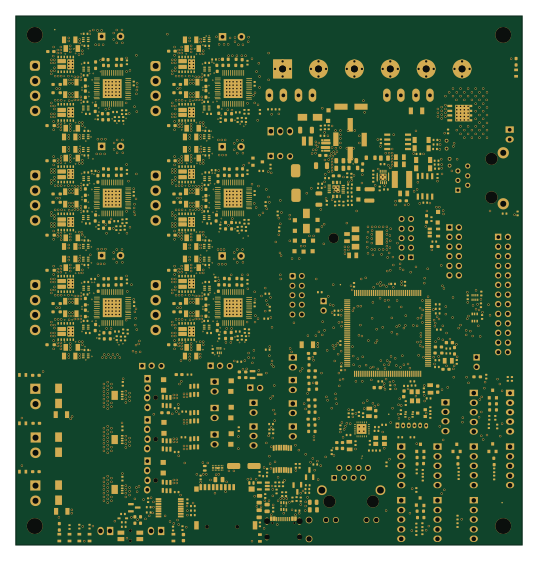 Microchip SAM
Duet3 MB 6HC
134 × 140 mm652 parts4LNo license0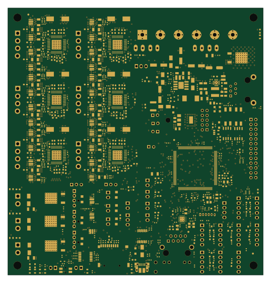 Microchip SAM
Duet3 MB
134 × 140 mm642 parts4LNo license0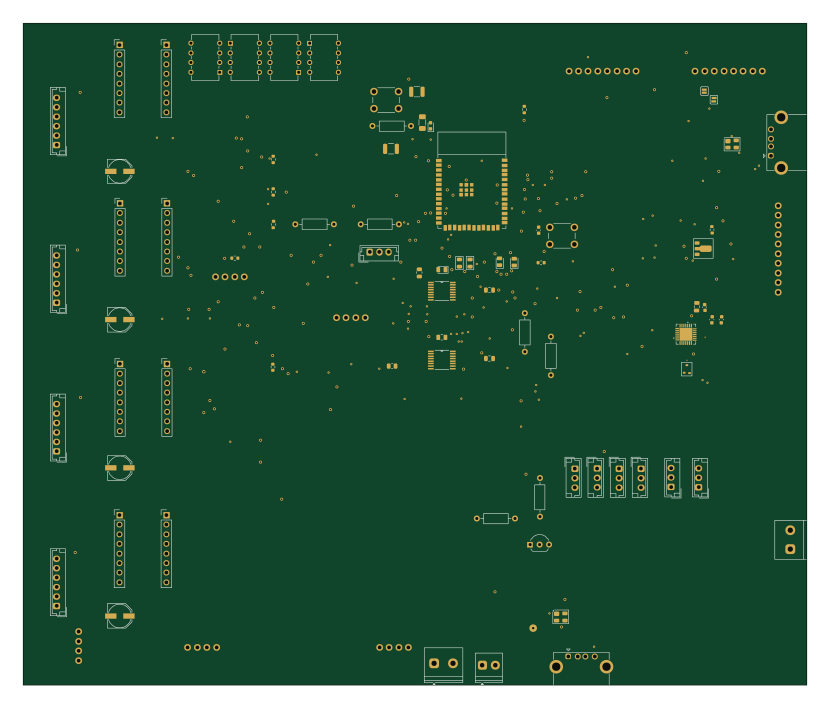 ESP32
ESP32Mainboard Layout No daisy chain cp2102 moved
207 × 174.8 mm87 parts2LNo license0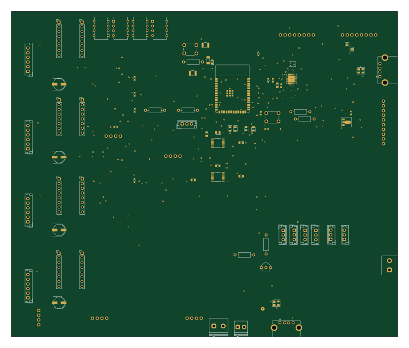 ESP32
ESP32Mainboard Layout No daisy chain
207 × 174.8 mm87 parts2LNo license0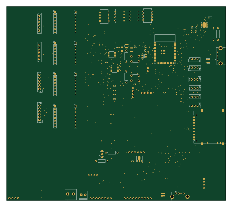 ESP32
ESP32Mainboard layout Pre-16 pin SD module
191.3 × 169.2 mm80 parts2LNo license0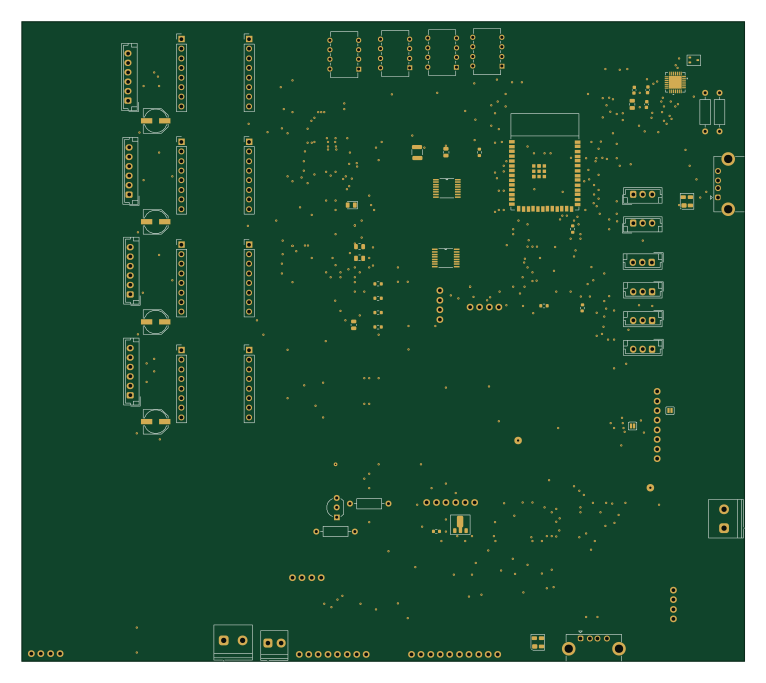 ESP32
ESP32Mainboard layout Daisy chain removed
191.3 × 169.2 mm74 parts2LNo license0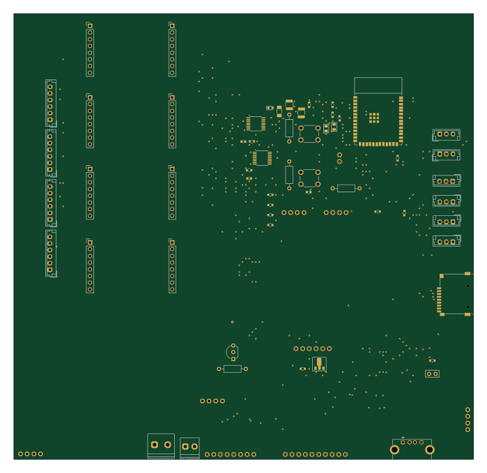 ESP32
ESP32Mainboard layout track size .5 mm swap
174.5 × 169.2 mm67 parts2LNo license0
Standalone DRV8825
38.7 × 23.3 mm19 parts2LNo license0
Standalone DRV8825 V1
35.6 × 26.7 mm15 parts2LNo license0
In case ghosting fails Standalone DRV8825
42.5 × 31.2 mm15 parts2LNo license0
LM2576 Var Volt Reg
48 × 48.2 mm14 parts2LNo license0
Earlier revisions in the repo: Mainboard layout
Similar boards
 ESP32
ESP32Open Book Abridged Edition
joeycastillo
85 × 115 mm65 parts2LCC-BY-SA-4.08.1k ESP32
ESP32Badge
atopile
56.3 × 39 mm239 parts4LMIT4.0k ESP32
ESP32Esp32 minimal
36.2 × 26.8 mm20 parts2LMIT4.0k ESP32
ESP32Racer
StuckAtPrototype
36 × 50.2 mm70 parts4LApache-2.03.8k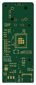 ESP32
ESP32Controller
29 × 74 mm58 parts4LApache-2.03.8k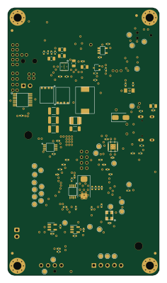 ESP32
ESP32Bitaxe
skot
56.5 × 99.8 mm86 parts4LCERN-OHL-S-2.01.4k