
KiCadPlatine

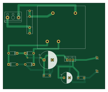
About the KiCadPlatine PCB
KiCadPlatine is an open source PCB design by RwHexa, published on GitHub under the MIT license. It is a 2-layer board measuring 92 × 77 mm, with 14 components from 11 distinct parts.
Other key parts include the LM7812. By type, the board carries 4 diodes, 4 capacitors, 2 jumpers, 1 IC, 1 connector and 1 fuse.
It belongs with the power & battery designs in this gallery.
From the project
Netzteil 230V~ auf +12V (7812) - Schaltplan, Layout und Produktionsdaten vollstaendig von der KI Claude entwickelt. KiCad 8, ERC/DRC 0 Verstoesse.
KiCad-8-Projekt nach dem Referenz-Schaltbild: Printtrafo TR1 → Brückengleichrichter aus 4 × 1N4007 → Siebung C1/C2 → Festspannungsregler LM7812 → C3/C4 → Ausgangsklemmen JP1 (+12 V) und JP2 (0 V = GND).
Die Platine ist vollständig geroutet (50 Leiterbahnsegmente, 2 Durchkontaktierungen) und hat eine gefüllte Massefläche auf der Rückseite — ausschließlich auf der Sekundärseite, damit unter den netzspannungsführenden Bahnen kein Kupfer liegt.
Main components on the KiCadPlatine
KiCadPlatine bill of materials (BOM)
14 components, 11 distinct parts — part numbers from the project's BOM.
| Qty | Part | Footprint | Refs |
|---|---|---|---|
| 1 | LM7812 | TO-220-3_Vertical | U1 |
| 1 | 230V~ L/N | TerminalBlock_RND_205-00023_1x02_P10.00mm_Horizontal | J1 |
| 1 | T 160mA / 250V | Fuseholder_Clip-5x20mm_Littelfuse_111_Inline_P20.00x5.00mm_D1.05mm_Horizontal | F1 |
| 1 | DC OUT z.B. +12V | PinHeader_1x01_P2.54mm_Vertical | JP1 |
| 1 | 0V = GND | PinHeader_1x01_P2.54mm_Vertical | JP2 |
| 1 | 230V/15V 15VA | Trafo_Print_15VA_4pin | TR1 |
| 4 | 1N4007 | D_DO-41_SOD81_P7.62mm_Horizontal | D1, D2, D3, D4 |
| 1 | 2200UF/35V 2200uF/35V | CP_Radial_D16.0mm_P7.50mm | C1 |
| 1 | 100NF/100V 100nF/100V | C_Rect_L7.0mm_W2.5mm_P5.00mm | C2 |
| 1 | 100NF/50V 100nF/50V | C_Rect_L7.0mm_W2.5mm_P5.00mm | C3 |
| 1 | 100UF/25V 100uF/25V | CP_Radial_D10.0mm_P5.00mm | C4 |
KiCadPlatine design files
The KiCad project lives in the RwHexa/KiCadPlatine repository on GitHub; these links point at the commit this page was built from.
KiCadPlatine: common questions
How big is the KiCadPlatine PCB?
The KiCadPlatine measures 92 × 77 mm, has 2 copper layers and is 1.6 mm thick.
How many components are on the KiCadPlatine?
14 components, from 11 distinct parts, with part numbers taken from the project's own BOM. The full bill of materials is listed on this page.
Where can I download the KiCadPlatine design files?
From the RwHexa/KiCadPlatine repository on GitHub, which has the KiCad layout, the schematic and the BOM; the links under Design files point to each one.
Can I use the KiCadPlatine design in my own project?
Yes, under the terms of its MIT license, which RwHexa chose for the repository.
Similar boards

Stack chan
stack-chan
50 × 50 mm33 parts2LApache-2.01.7k
Display Carrier
AxxAxx
35.6 × 58.2 mm5 parts2LGPL-3.01.7k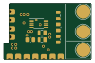
ControllerCurrentShuntAddOn
stuartpittaway
26 × 16.9 mm9 parts2LCC-BY-NC-4.01.1k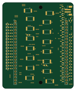
Module 16S PassiveBalanceAddOn
61 × 74 mm86 parts2LCC-BY-NC-4.01.1k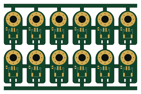
TemperaturePCB PANEL
116 × 75.5 mm178 parts2LCC-BY-NC-4.01.1k
ProgrammingAdapter
10.5 × 83 mm3 parts2LCC-BY-NC-4.01.1k