
Twinusb

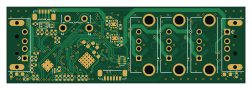
About the Twinusb PCB
Twinusb is an open source STM32 PCB design by s-t-e-f-a-n, published on GitHub. It is a 4-layer board measuring 63 × 20 mm, with 112 components from 31 distinct parts.
Its main chip is the STM32G0B1KBU6, from the STM32 family. Other key parts include the TPS2553DRVR-1, TPS2116DRLR, USBLC6-2P6, INA180B2IDBVR and GL852G-OHY60. By type, the board carries 48 capacitors, 43 resistors, 14 ICs, 2 connectors, 2 diodes and 1 transistor.
It belongs with the displays & leds and usb & debug tools designs in this gallery.
From the project
H₂H³ | Twin USB Host Switch × Triple USB Hub (with OLED Telemetry)
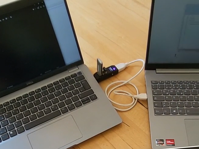
H₂H³ is a compact, STM32 microcontroller-driven USB 2.0 KVM switch and 3-port hub designed to maintain a clean, clutter-free workspace in modern home offices. It enables two computers to seamlessly share a single set of peripherals—like your keyboard, mouse, and flash drives—while delivering live voltage and current telemetry via an integrated OLED display. Paired with the native Rust host daemon, H₂H³ features seamless automatic host switching as your mouse reaches the screen edge, alongside intuitive configuration directly from your system tray.
Main components on the Twinusb
Twinusb bill of materials (BOM)
112 components, 31 distinct parts.
| Qty | Part | Footprint | Refs |
|---|---|---|---|
| 2 | TPS2553DRVR-1 Texas Instruments | WSON-6-1EP_2x2mm_P0.65mm_EP1x1.6mm_ThermalVias | U1, U2 |
| 1 | TPS2116DRLR TPS2116DRL Texas Instruments | SOT-583-8 | U3 |
| 5 | USBLC6-2P6 STMicroelectronics | SOT-666 | U4, U6, U8, U10, U14 |
| 3 | INA180B2IDBVR INA180B2, 50V/V Texas Instruments | SOT-23-5 | U5, U7, U9 |
| 1 | GL852G-OHY60 Genesys Logic | QFN-28-1EP_5x5mm_P0.5mm_EP3.75x3.75mm_ThermalVias | U11 |
| 1 | FSUSB42MUX onsemi | MSOP-10_3x3mm_P0.5mm | U12 |
| 1 | STM32G0B1KBU6 STM32G0B1KBUx STMicroelectronics | QFN-32-1EP_5x5mm_P0.5mm_EP3.45x3.45mm_ThermalVias | U13 |
| 1 | DMN62D0LFB Diodes | DFN1006-3 | Q1 |
| 1 | X322512MSB4SI 12M YXC | Crystal_SMD_3225-4Pin_3.2x2.5mm | Y1 |
| 1 | BM04B-SURS-TF 1x4, 0.8mm, Vertical, Receptable JST | JST_SUR_BM04B-SURS-TF_1x04-1MP_P0.80mm_Vertical | J2 |
| 1 | BM06B-SURS-TF 1x6, 0.8mm, Vertical, Receptable JST | JST_SUR_BM06B-SURS-TF_1x06-1MP_P0.80mm_Vertical | J3 |
| 1 | APHF1608LSEEQBDZGKC LED_ARBG Kingbright | LED_RGB_Kingbright_APHF1608LSEEQBDZGKC | D1 |
| 1 | BAT54LP Diodes | Diodes_DFN1006-2 | D2 |
| 1 | MLZ1608N100LTD25 10u, 60 mA TDK | L_0603_1608Metric | L1 |
| 5 | 4n7 | C_0603_1608Metric | C1, C13, C15, C20, C25 |
| 24 | 100n | C_0402_1005Metric | C2, C9, C11, C14, C17, C19, C22, C24 +16 |
| 6 | 10n | C_0402_1005Metric | C3, C4, C5, C6, C44, C46 |
| 6 | 10u | C_0603_1608Metric | C7, C8, C18, C23, C28, C48 |
| 2 | 1u | C_0402_1005Metric | C10, C12 |
| 3 | T520A107M006ATE070 100u 6V3 Tantal Polymer Kemet | CP_EIA-3216-18_Kemet-A | C16, C21, C26 |
Show 11 more
| Qty | Part | Footprint | Refs |
|---|---|---|---|
| 2 | 22p | C_0402_1005Metric | C29, C30 |
| 2 | 1M | R_0402_1005Metric | R1, R23 |
| 10 | 10k | R_0402_1005Metric | R2, R3, R4, R5, R10, R11, R33, R36 +2 |
| 2 | 240R | R_0402_1005Metric | R6, R7 |
| 4 | 470R | R_0402_1005Metric | R8, R27, R28, R31 |
| 4 | 1k | R_0402_1005Metric | R9, R13, R16, R17 |
| 11 | 100k | R_0402_1005Metric | R12, R14, R15, R20, R29, R30, R34, R35 +3 |
| 2 | 16k9 | R_0402_1005Metric | R21, R22 |
| 3 | PE0603FRF7T0R039L 39m, 1%, 100ppm/K Yageo | R_0603_1608Metric | R24, R25, R26 |
| 1 | 680R | R_0402_1005Metric | R32 |
| 4 | 4k7 | R_0402_1005Metric | R42, R43, R44, R45 |
Twinusb design files
The KiCad project lives in the s-t-e-f-a-n/twinusb repository on GitHub; these links point at the commit this page was built from.
Twinusb: common questions
What microcontroller does the Twinusb use?
The Twinusb is built around the STM32G0B1KBU6, from the STM32 family.
How big is the Twinusb PCB?
The Twinusb measures 63 × 20 mm, has 4 copper layers and is 1.5842 mm thick.
How many components are on the Twinusb?
112 components, from 31 distinct parts. The full bill of materials is listed on this page.
Where can I download the Twinusb design files?
From the s-t-e-f-a-n/twinusb repository on GitHub, which has the KiCad layout and the schematic; the links under Design files point to each one.
Can I use the Twinusb design in my own project?
The repository has no license, so all rights stay with s-t-e-f-a-n. Use it as a reference, and ask the author before reusing the design.
Can I test firmware for the Twinusb without the hardware?
Yes. HardLabs builds a simulation of the board from its netlist and BOM, so you can run and debug STM32 firmware against it before you order a PCB.
Similar boards
 STM32
STM32LumenPnP Motherboard
opulo-inc
149 × 95 mm296 parts4LCC-BY-SA-4.03.7k STM32
STM32AxxSolder
AxxAxx
39 × 82.5 mm122 parts2LGPL-3.01.7k STM32
STM32AIOC
skuep
21 × 31.5 mm47 parts2LMIT1.4k STM32
STM32Ferris
pierrechevalier83
208.8 × 86.8 mm102 parts2LSHL-2.11.3k STM32
STM32176 pin board
rusefi
61.8 × 73.2 mm76 parts2LGPL-3.01.2k STM32
STM32Brain board STM32F407
61.8 × 73.2 mm69 parts2LGPL-3.01.2k