
Buck boost converter

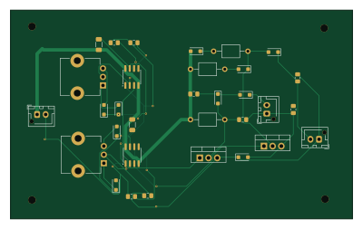
About the Buck boost converter PCB
Buck boost converter is an open source PCB design by sachinp-engineer, published on GitHub under the MIT license. It is a 2-layer board measuring 99.8 × 61 mm, with 32 components from 8 distinct parts.
Other key parts include the LM555xM. By type, the board carries 10 diodes, 8 capacitors, 3 connectors, 3 inductors, 2 ICs and 2 transistors.
It belongs with the power & battery designs in this gallery.
From the project
A collection of PCB design projects created using KiCad. This repository contains schematic designs, PCB layouts, 3D renders, and manufacturing files for various electronics projects.
A PCB implementation of a DC-DC Buck-Boost Converter designed using KiCad.
This converter can either increase (boost) or decrease (buck) the input voltage depending on the operating conditions.
- Dual PWM Signal Generator using LM555 Timer ICs - Buck-Boost Converter Stage - MOSFET Switching Circuit - Compact PCB Layout - 3D PCB Design
- KiCad 9 - PCB Editor - Schematic Editor - 3D Viewer
Main components on the Buck boost converter
Buck boost converter bill of materials (BOM)
32 components, 8 distinct parts.
| Qty | Part | Footprint | Refs |
|---|---|---|---|
| 2 | LM555xM | SOIC-8_3.9x4.9mm_P1.27mm | U1, U2 |
| 2 | IRF540N | TO-220-3_Vertical | Q1, Q3 |
| 3 | Conn_01x02_Pin | JST_XH_B2B-XH-AM_1x02_P2.50mm_Vertical | J1, J2, J3 |
| 2 | R_Potentiometer | Potentiometer_TT_P0915N | RV1, RV2 |
| 10 | D | D_SOD-123F | D1, D2, D3, D4, D5, D6, D7, D8 +2 |
| 3 | L | L_Axial_L5.0mm_D3.6mm_P10.00mm_Horizontal_Murata_BL01RN1A2A2 | L1, L2, L3 |
| 8 | C | C_0805_2012Metric_Pad1.18x1.45mm_HandSolder | C1, C2, C3, C4, C5, C6, C7, C8 |
| 2 | R | R_1206_3216Metric_Pad1.30x1.75mm_HandSolder | R1, R4 |
Buck boost converter design files
The KiCad project lives in the sachinp-engineer/PCB-Projects repository on GitHub; these links point at the commit this page was built from.
Buck boost converter: common questions
How big is the Buck boost converter PCB?
The Buck boost converter measures 99.8 × 61 mm, has 2 copper layers and is 1.6 mm thick.
How many components are on the Buck boost converter?
32 components, from 8 distinct parts. The full bill of materials is listed on this page.
Where can I download the Buck boost converter design files?
From the sachinp-engineer/PCB-Projects repository on GitHub, which has the KiCad layout and the schematic; the links under Design files point to each one.
Can I use the Buck boost converter design in my own project?
Yes, under the terms of its MIT license, which sachinp-engineer chose for the repository.
More boards in PCB-Projects
Similar boards
EinkPDA screen
TalismanDesign
95 × 54 mm27 parts2LApache-2.02.0k
Stack chan
stack-chan
50 × 50 mm33 parts2LApache-2.01.7k
Display Carrier
AxxAxx
35.6 × 58.2 mm5 parts2LGPL-3.01.7k
Module 16S PassiveBalanceAddOn
stuartpittaway
61 × 74 mm86 parts2LCC-BY-NC-4.01.1k
TemperaturePCB PANEL
116 × 75.5 mm178 parts2LCC-BY-NC-4.01.1k
ProgrammingAdapter
10.5 × 83 mm3 parts2LCC-BY-NC-4.01.1k