
ADS1015 ADC


About the ADS1015 ADC PCB
ADS1015 ADC is an open source PCB design by SolderedElectronics, published on GitHub under the TAPR-OHL-1.0 license. It is a 2-layer board measuring 22 × 22 mm, with 17 components from 13 distinct parts.
Other key parts include the ADS1115. By type, the board carries 5 jumpers, 5 relays, 3 resistors, 1 IC and 1 capacitor.
It belongs with the dev boards & breakouts designs in this gallery.
From the project
Hardware design, BOM, gerbers and 3D files for ADC-12-bit-ADS1015-4-channel-with-PGA-breakout designed by Soldered Electronics.
ADC (Analog Digital Converter) is a device that reads analog signals (just like the analogRead () function in Arduino IDE) and converts them into digital signals that can be read by a microcontroller. This breakout is based on the ADS1015 ADC, which reads values in 12-bit resolution, receives a maximum of 3.3V on its inputs and has a total of 4 channels (which can also be used as two differential). Works great with any microcontroller at 5V. It has 2 easyC connectors for easier connection on I2C communication.

Main components on the ADS1015 ADC
ADS1015 ADC bill of materials (BOM)
17 components, 13 distinct parts — part numbers from the project's BOM.
| Qty | Part | Footprint | Refs |
|---|---|---|---|
| 1 | ADS1115 | VSSOP | U1 |
| 2 | HOLE_3.2MM HOLE_3.2mm | HOLE_3.2mm | H1, H2 |
| 1 | SMD_JUMPER_3_PAD_TRACE | SMD_JUMPER_3_PAD_TRACE | JP1 |
| 1 | 0X48 0x48 | SMD_JUMPER_CONNECTED | JP2 |
| 1 | 0X49 0x49 | SMD_JUMPER | JP3 |
| 1 | 0X4A 0x4A | SMD_JUMPER | JP4 |
| 1 | 0X4B 0x4B | SMD_JUMPER | JP5 |
| 1 | HEADER_MALE_5X1 | HEADER_MALE_5X1 | K1 |
| 1 | HEADER_MALE_4X1 | HEADER_MALE_4X1 | K2 |
| 2 | easyC-SMD | easyC-connector | K3, K4 |
| 1 | HEADER_MALE_1X1 | HEADER_MALE_1X1 | K5 |
| 1 | 0.1UF 0.1uF | 0603C | C1 |
| 3 | 10K 10k | 0603R | R1, R2, R3 |
ADS1015 ADC design files
The KiCad project lives in the SolderedElectronics/ADC-12-bit-ADS1015-4-channel-with-PGA-breakout-hardware-design repository on GitHub; these links point at the commit this page was built from.
ADS1015 ADC: common questions
How big is the ADS1015 ADC PCB?
The ADS1015 ADC measures 22 × 22 mm, has 2 copper layers and is 1.6 mm thick.
How many components are on the ADS1015 ADC?
17 components, from 13 distinct parts, with part numbers taken from the project's own BOM. The full bill of materials is listed on this page.
Where can I download the ADS1015 ADC design files?
From the SolderedElectronics/ADC-12-bit-ADS1015-4-channel-with-PGA-breakout-hardware-design repository on GitHub, which has the KiCad layout, the schematic and the BOM; the links under Design files point to each one.
Can I use the ADS1015 ADC design in my own project?
Yes, under the terms of its TAPR-OHL-1.0 license, which SolderedElectronics chose for the repository.
More boards in ADC-12-bit-ADS1015-4-channel-with-PGA-breakout-hardware-design

Similar boards
Breakout 112pin Connector
rusefi
174 × 58 mm39 parts2LGPL-3.01.2k
Eecv breakout
140.8 × 53.7 mm9 parts4LGPL-3.01.2k
Breakout 60pin EEC-IV
139.7 × 62.2 mm15 parts2LGPL-3.01.2k
134pin 7-967288-1
139.7 × 73.7 mm38 parts2LGPL-3.01.2k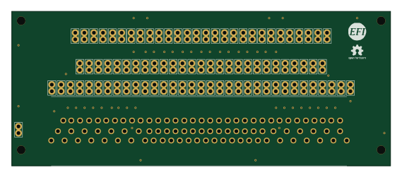
88 Pin Vag Breakout
142 × 58 mm91 parts2LGPL-3.01.2k
Rj45 breakout
rene-dev
15.2 × 53.8 mm3 parts2LGPL-3.0979