
Sony mhc gn1300d-5.1-revival

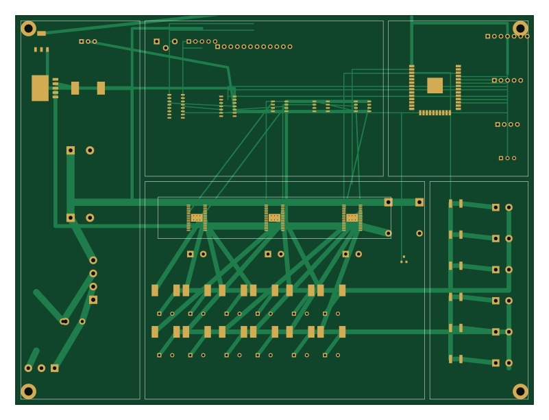
About the Sony mhc gn1300d-5.1-revival PCB
Sony mhc gn1300d-5.1-revival is an open source PCB design by stsukesh, published on GitHub under the MIT license. It is a 2-layer board measuring 200 × 150 mm, with 40 components from 15 distinct parts.
By type, the board carries 12 inductors, 2 capacitors, 1 transistor, 1 fuse and 1 relay.
It belongs with the audio, iot & wireless and power & battery designs in this gallery.
From the project
Complete DIY/OEM revival of Sony MHC-GN1300D 5.1 audio system: custom KiCad 10 PCB (Lion Circuits), 3x TPA3116D2, analog crossover, and ESP32 IoT control hub.
A complete, production-grade revival and modernization system for the vintage Sony MHC-GN1300D Mini Hi-Fi Component System (and similar 5.1 home theater units).
This project replaces dead, obsolete hybrid IC amplifier boards (STK modules) and failing logic boards with a single custom 150×200mm 2-layer PCB, modern high-efficiency Class-D amplification, an active analog crossover, an ESP32 IoT control hub, and a multi-layer hardware-software fail-proof protection engine.
Sony mhc gn1300d-5.1-revival bill of materials (BOM)
40 components, 15 distinct parts — part numbers from the project's BOM.
| Qty | Part | Footprint | Refs |
|---|---|---|---|
| 1 | 2N2222 | SOT-23 | Q1 |
| 1 | KBU810 KBU810_8A | Diode_Bridge_Vishay_KBU | BR1 |
| 3 | — | CP_Radial_D12.5mm_P5.00mm | C_BULK1, C_BULK2, C_BULK3 |
| 12 | — | C_Rect_L7.2mm_W4.5mm_P5.00mm_FKS2_FKP2_MKS2_MKP2 | C_O1, C_O2, C_O3, C_O4, C_O5, C_O6, C_O7, C_O8 +4 |
| 1 | 3A_250V | Fuseholder_5x20mm | F1 |
| 1 | SRD-05VDC-SL-C RELAY_10A_24V | Relay_SPST_SANYOU_SRD_Series_Form_A | K1 |
| 1 | 14D431K | RV_Disc_D14mm_W4.5mm_P7.5mm | RV1 |
| 1 | TPA3116_FL_FR | HTSSOP-32-1EP_6.1x11mm_P0.65mm_EP3.1x6.1mm_ThermalVias | U_AMP1 |
| 1 | TPA3116_SL_SR | HTSSOP-32-1EP_6.1x11mm_P0.65mm_EP3.1x6.1mm_ThermalVias | U_AMP2 |
| 1 | TPA3116_C_SUB | HTSSOP-32-1EP_6.1x11mm_P0.65mm_EP3.1x6.1mm_ThermalVias | U_AMP3 |
| 1 | NE5532_HPF | SOIC-8_3.9x4.8mm_P1.27mm | U_OP1 |
| 1 | NE5532_SUM | SOIC-8_3.9x4.8mm_P1.27mm | U_OP2 |
| 1 | NE5532_LPF_C | SOIC-8_3.9x4.8mm_P1.27mm | U_OP3 |
| 12 | 22uH_5A | L_10.4x10.4_H4.8 | L1, L2, L3, L4, L5, L6, L7, L8 +4 |
| 2 | 4700uF_35V | CP_Radial_D18.0mm_P7.50mm | C1, C2 |
Sony mhc gn1300d-5.1-revival design files
The KiCad project lives in the stsukesh/sony-mhc-gn1300d-5.1-revival repository on GitHub; these links point at the commit this page was built from.
Sony mhc gn1300d-5.1-revival: common questions
How big is the Sony mhc gn1300d-5.1-revival PCB?
The Sony mhc gn1300d-5.1-revival measures 200 × 150 mm, has 2 copper layers and is 1.6 mm thick.
How many components are on the Sony mhc gn1300d-5.1-revival?
40 components, from 15 distinct parts, with part numbers taken from the project's own BOM. The full bill of materials is listed on this page.
Where can I download the Sony mhc gn1300d-5.1-revival design files?
From the stsukesh/sony-mhc-gn1300d-5.1-revival repository on GitHub, which has the KiCad layout, the schematic and the BOM; the links under Design files point to each one.
Can I use the Sony mhc gn1300d-5.1-revival design in my own project?
Yes, under the terms of its MIT license, which stsukesh chose for the repository.
Similar boards

Stack chan
stack-chan
50 × 50 mm33 parts2LApache-2.01.7k
Display Carrier
AxxAxx
35.6 × 58.2 mm5 parts2LGPL-3.01.7k
KLOR
GEIGEIGEIST
160.2 × 118.3 mm79 parts2LGPL-3.01.2k
ControllerCurrentShuntAddOn
stuartpittaway
26 × 16.9 mm9 parts2LCC-BY-NC-4.01.1k
Module 16S PassiveBalanceAddOn
61 × 74 mm86 parts2LCC-BY-NC-4.01.1k
TemperaturePCB PANEL
116 × 75.5 mm178 parts2LCC-BY-NC-4.01.1k