
Capacitive-Pattern-Based-Input-Lock

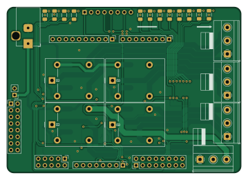
About the Capacitive-Pattern-Based-Input-Lock PCB
Capacitive-Pattern-Based-Input-Lock is an open source PCB design by Tai-Min, published on GitHub under the MIT license. It is a 2-layer board measuring 89.7 × 63.4 mm, with 58 components from 18 distinct parts.
Other key parts include the 74HC595. By type, the board carries 20 resistors, 16 diodes, 13 connectors, 4 transistors, 4 relays and 1 IC.
It belongs with the dev boards & breakouts, iot & wireless and sensors designs in this gallery.
From the project
Reinvent low power user's input using PSoC4100s reliable capticive technology combined with machine learning
Created for Propel Human-Machine Interactions into the Future with Infineon. For the detailed description of the project see Capacitive Pattern Based Input Lock on Hackster.io
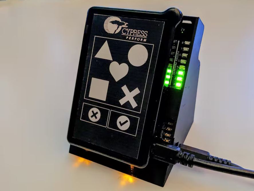
Main components on the Capacitive-Pattern-Based-Input-Lock
Capacitive-Pattern-Based-Input-Lock bill of materials (BOM)
58 components, 18 distinct parts.
| Qty | Part | Footprint | Refs |
|---|---|---|---|
| 1 | 74HC595 | SOP-16_4.55x10.3mm_P1.27mm | U1 |
| 4 | BC847 | TSOT-23 | Q1, Q2, Q3, Q4 |
| 1 | 12V_IN | BarrelJack_Horizontal | J1 |
| 1 | EXT_PWR | PinHeader_1x02_P2.54mm_Vertical | J2 |
| 4 | Conn_01x03 | TerminalBlock_Phoenix_MKDS-1,5-3-5.08_1x03_P5.08mm_Horizontal | J3, J4, J7, J8 |
| 1 | KitProg2_PROG | PinHeader_2x05_P2.54mm_Vertical | J5 |
| 1 | KitProg2_IO | PinHeader_2x08_P2.54mm_Vertical | J6 |
| 1 | UNO_7_0 | PinHeader_1x08_P2.54mm_Vertical | J9 |
| 1 | UNO_13_8 | PinHeader_1x10_P2.54mm_Vertical | J10 |
| 1 | DEBUG_OLED | PinSocket_1x08_P2.54mm_Vertical | J11 |
| 1 | UNO_PWR | PinHeader_1x08_P2.54mm_Vertical | J12 |
| 1 | UNO_A0_A5 | PinHeader_2x08_P2.54mm_Vertical | J13 |
| 4 | G5LE-1 | Relay_SPDT_Omron-G5LE-1 | K1, K2, K3, K4 |
| 12 | LED | LED_1206_3216Metric_Pad1.42x1.75mm_HandSolder | D1, D2, D5, D6, D7, D8, D9, D10 +4 |
| 4 | D | D_SMC_Handsoldering | D3, D4, D11, D12 |
| 12 | 220 | R_1206_3216Metric_Pad1.30x1.75mm_HandSolder | R1, R2, R7, R8, R9, R10, R11, R14 +4 |
| 4 | 1k | R_1206_3216Metric_Pad1.30x1.75mm_HandSolder | R3, R4, R12, R13 |
| 4 | 10k | R_1206_3216Metric_Pad1.30x1.75mm_HandSolder | R5, R6, R15, R16 |
Capacitive-Pattern-Based-Input-Lock design files
The KiCad project lives in the Tai-Min/Capacitive-Pattern-Based-Input-Lock repository on GitHub; these links point at the commit this page was built from.
- Layoutshield/shield.kicad_pcb
- Schematicshield/shield.kicad_sch
Capacitive-Pattern-Based-Input-Lock: common questions
How big is the Capacitive-Pattern-Based-Input-Lock PCB?
The Capacitive-Pattern-Based-Input-Lock measures 89.7 × 63.4 mm, has 2 copper layers and is 1.6 mm thick.
How many components are on the Capacitive-Pattern-Based-Input-Lock?
58 components, from 18 distinct parts. The full bill of materials is listed on this page.
Where can I download the Capacitive-Pattern-Based-Input-Lock design files?
From the Tai-Min/Capacitive-Pattern-Based-Input-Lock repository on GitHub, which has the KiCad layout and the schematic; the links under Design files point to each one.
Can I use the Capacitive-Pattern-Based-Input-Lock design in my own project?
Yes, under the terms of its MIT license, which Tai-Min chose for the repository.
Similar boards
Sensor smd
scottbez1
40 × 20 mm5 parts2LApache-2.04.2k
Sensors
StuckAtPrototype
15.2 × 9 mm14 parts4LApache-2.03.8k
Microphone
Mentra-Community
5.5 × 6.1 mm6 parts2LMIT1.2k
Eecv breakout
rusefi
140.8 × 53.7 mm9 parts4LGPL-3.01.2k
134pin 7-967288-1
139.7 × 73.7 mm38 parts2LGPL-3.01.2k
Breakout 60pin EEC-IV
139.7 × 62.2 mm15 parts2LGPL-3.01.2k