
Hands-On-PCB-Engineering-HOPE-

About the Hands-On-PCB-Engineering-HOPE-
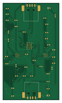
Hands-On-PCB-Engineering-HOPE- is an open source PCB design by tatendajoes, published on GitHub. It is a 2-layer board measuring 51 × 87 mm, with 40 components from 20 distinct parts.
Other key parts include the LM73605QRNPTQ1 and TPS2549RTER. By type, the board carries 19 capacitors, 13 resistors, 3 ICs, 2 connectors, 2 diodes and 1 inductor.
It belongs with the power & battery and sensors designs in this gallery.
From the project
- Schematic Diagram !shematic diagram of USB charger PCB
- Schematic Diagram !shematic diagram of USB charger PCB
- PCB Diagram !pcb diagram of USB charger PCB
Main components on the Hands-On-PCB-Engineering-HOPE-
Hands-On-PCB-Engineering-HOPE- bill of materials (BOM)
40 components, 20 distinct parts.
| Qty | Part | Footprint | Refs |
|---|---|---|---|
| 1 | LM73605QRNPTQ1 | RNP0030A | U1 |
| 2 | TPS2549RTER | RTE0016C | U2, U3 |
| 2 | USB CONN | CUI_UJ2-AH-1-SMT | J1, J2 |
| 2 | LED_Filled | D_0603_1608Metric_Pad1.05x0.95mm_HandSolder | D1, D2 |
| 1 | 6.8uH | L_0603_1608Metric_Pad1.05x0.95mm_HandSolder | L1 |
| 3 | 0.47uF | C_0603_1608Metric_Pad1.08x0.95mm_HandSolder | C1, C5, C12 |
| 5 | 10uF | C_0603_1608Metric_Pad1.08x0.95mm_HandSolder | C2, C3, C4, C17, C18 |
| 6 | 47uF | C_0603_1608Metric_Pad1.08x0.95mm_HandSolder | C6, C7, C8, C9, C10, C11 |
| 1 | 0.022uF | C_0603_1608Metric_Pad1.08x0.95mm_HandSolder | C13 |
| 3 | 0.1uF | C_0603_1608Metric_Pad1.08x0.95mm_HandSolder | C14, C15, C16 |
| 1 | 2.2uF | C_0603_1608Metric_Pad1.08x0.95mm_HandSolder | C19 |
| 1 | 2.1K | R_0603_1608Metric_Pad0.98x0.95mm_HandSolder | R1 |
| 1 | 112K | R_0603_1608Metric_Pad0.98x0.95mm_HandSolder | R2 |
| 1 | 3.0R | R_0603_1608Metric_Pad0.98x0.95mm_HandSolder | R3 |
| 3 | 0R | R_0603_1608Metric_Pad0.98x0.95mm_HandSolder | R4, R8, R9 |
| 1 | 47K | R_0603_1608Metric_Pad0.98x0.95mm_HandSolder | R5 |
| 1 | 200K | R_0603_1608Metric_Pad0.98x0.95mm_HandSolder | R6 |
| 1 | 10K | R_0603_1608Metric_Pad0.98x0.95mm_HandSolder | R7 |
| 2 | 20K | R_0603_1608Metric_Pad0.98x0.95mm_HandSolder | R10, R11 |
| 2 | 715 | R_0603_1608Metric_Pad0.98x0.95mm_HandSolder | R12, R13 |
Hands-On-PCB-Engineering-HOPE- design files
The KiCad project lives in the tatendajoes/Hands-On-PCB-Engineering-HOPE- repository on GitHub; these links point at the commit this page was built from.
Hands-On-PCB-Engineering-HOPE-: common questions
How big is the Hands-On-PCB-Engineering-HOPE-?
The Hands-On-PCB-Engineering-HOPE- measures 51 × 87 mm, has 2 copper layers and is 1.6 mm thick.
How many components are on the Hands-On-PCB-Engineering-HOPE-?
40 components, from 20 distinct parts. The full bill of materials is listed on this page.
Where can I download the Hands-On-PCB-Engineering-HOPE- design files?
From the tatendajoes/Hands-On-PCB-Engineering-HOPE- repository on GitHub, which has the KiCad layout and the schematic; the links under Design files point to each one.
Can I use the Hands-On-PCB-Engineering-HOPE- design in my own project?
The repository has no license, so all rights stay with tatendajoes. Use it as a reference, and ask the author before reusing the design.
Similar boards
Sensor smd
scottbez1
40 × 20 mm5 parts2LApache-2.04.2k
Sensors
StuckAtPrototype
15.2 × 9 mm14 parts4LApache-2.03.8k
EinkPDA screen
TalismanDesign
95 × 54 mm27 parts2LApache-2.02.0k
Stack chan
stack-chan
50 × 50 mm33 parts2LApache-2.01.7k
Display Carrier
AxxAxx
35.6 × 58.2 mm5 parts2LGPL-3.01.7k
Microphone
Mentra-Community
5.5 × 6.1 mm6 parts2LMIT1.2k