
Task 1

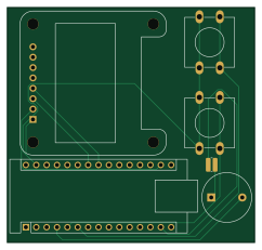
About the Task 1 PCB
Task 1 is an open source AVR/Arduino PCB design by teamantariksh-satellites, published on GitHub. It is a 2-layer board measuring 60.5 × 57.5 mm, with 6 components from 5 distinct parts.
Its main chip is the Arduino_Nano_v3.x, from the AVR/Arduino family. Other key parts include the ER_OLEDM0.91_1x-I2C. By type, the board carries 2 switches, 1 IC, 1 module, 1 buzzer and 1 resistor.
It belongs with the displays & leds designs in this gallery.
From the project
This circuit is a simple interactive embedded system based on an Arduino Nano. It features a 0.91-inch I2C OLED display for visual feedback, two push buttons for user input, and a buzzer for audio signaling. It serves as a foundational platform for menu-based interfaces, basic ga
This circuit is a simple interactive embedded system based on an Arduino Nano. It features a 0.91-inch I2C OLED display for visual feedback, two push buttons for user input, and a buzzer for audio signaling. It serves as a foundational platform for menu-based interfaces, basic games, or alert systems.
Display: The OLED uses the standard I2C bus, with SDA connected to A4 and SCL connected to A5. Inputs: SW1 and SW2 connect to digital pins D2 and D3, respectively. The schematic lacks external pull-up resistors; therefore, the microcontroller's internal pull-ups must be enabled in firmware…
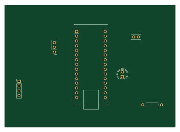
Main components on the Task 1
Task 1 bill of materials (BOM)
6 components, 5 distinct parts.
| Qty | Part | Footprint | Refs |
|---|---|---|---|
| 1 | ER_OLEDM0.91_1x-I2C | Adafruit_SSD1306 | U1 |
| 1 | Arduino_Nano_v3.x | Arduino_Nano | A1 |
| 1 | Buzzer | Buzzer_12x9.5RM7.6 | BZ1 |
| 2 | SW_Push | SW_PUSH-12mm | SW1, SW2 |
| 1 | 1k | R_0612_1632Metric_Pad1.18x3.40mm_HandSolder | R1 |
Task 1 design files
The KiCad project lives in the teamantariksh-satellites/PCB-design-training repository on GitHub; these links point at the commit this page was built from.
Task 1: common questions
What microcontroller does the Task 1 use?
The Task 1 is built around the Arduino_Nano_v3.x, from the AVR/Arduino family.
How big is the Task 1 PCB?
The Task 1 measures 60.5 × 57.5 mm, has 2 copper layers and is 1.6 mm thick.
How many components are on the Task 1?
6 components, from 5 distinct parts. The full bill of materials is listed on this page.
Where can I download the Task 1 design files?
From the teamantariksh-satellites/PCB-design-training repository on GitHub, which has the KiCad layout and the schematic; the links under Design files point to each one.
Can I use the Task 1 design in my own project?
The repository has no license, so all rights stay with teamantariksh-satellites. Use it as a reference, and ask the author before reusing the design.
Can I test firmware for the Task 1 without the hardware?
Yes. HardLabs builds a simulation of the board from its netlist and BOM, so you can run and debug AVR/Arduino firmware against it before you order a PCB.
More boards in PCB-design-training
Similar boards
 AVR/Arduino
Magspoof
samyk
35 × 29 mm11 parts2LNo license4.2k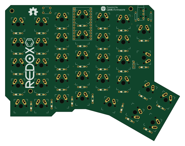 AVR/Arduino
Redox keyboard
mattdibi
162.2 × 126.5 mm77 parts2LMIT2.0k AVR/Arduino
Labrador
espotek-org
36.8 × 34.7 mm75 parts2LNo license1.2k AVR/Arduino
ModuleV450
stuartpittaway
30 × 61.4 mm39 parts2LCC-BY-NC-4.01.1k AVR/Arduino
V4
30 × 50 mm38 parts2LCC-BY-NC-4.01.1k AVR/Arduino
Discipline
coseyfannitutti
304.9 × 122.8 mm170 parts2LCC-BY-NC-4.01.0k