
PCB Laser Exposer II

About the PCB Laser Exposer II
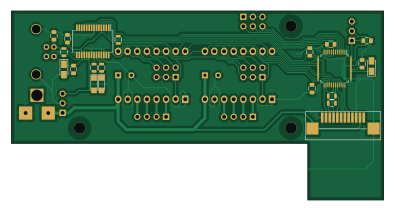
PCB Laser Exposer II is an open source TI MSP430/CC PCB design by terjeio, published on GitHub under the CERN-OHL-1.2 license. It is a 2-layer board measuring 98.5 × 50 mm, with 34 components from 23 distinct parts.
Its main chip is the MSP430F5310-48, from the TI MSP430/CC family. Other key parts include the FT232RL and POLOLU_A4988. By type, the board carries 12 capacitors, 10 connectors, 5 resistors, 4 ICs, 2 diodes and 1 inductor.
From the project
Mechanical and electrical design files for revised version of my PCB Laser exposer
160 x 100mm exposure area \(Eurocard\). Able to render at least down to 0.25mm \(10 mil, 250um\) track/track separation. Easy workflow.
Vector plotting requires parsing of a vector format to control the drive mechanism, most PCB-design packages are able to output the design in Gerber and/or HPGL-formats.
Raster plotting is similar to inkjet printing, the laser is fired for the individual pixels.
Main components on the PCB Laser Exposer II
PCB Laser Exposer II bill of materials (BOM)
34 components, 23 distinct parts.
| Qty | Part | Footprint | Refs |
|---|---|---|---|
| 1 | FT232RL | SSOP-28_5.3x10.2mm_Pitch0.65mm | U1 |
| 1 | MSP430F5310-48 | TQFP-48_7x7mm_Pitch0.5mm | U2 |
| 2 | POLOLU_A4988 | Polulu_A4988 | U3, U4 |
| 1 | 12V DC | BARREL_JACK | CON1 |
| 1 | SWPOWER | Pin_Header_Straight_1x03_Pitch2.54mm | P1 |
| 1 | USB_B | USB_B | P2 |
| 3 | CONN_02X03 | Pin_Header_Straight_2x03_Pitch2.54mm | P3, P8, P9 |
| 1 | CONN_01X14 | MOLEX_52271-1279 | P4 |
| 1 | PGM | Pin_Header_Straight_1x03_Pitch2.54mm | P5 |
| 1 | XAXIS | Pin_Header_Straight_1x04_Pitch2.54mm | P6 |
| 1 | YAXIS | Pin_Header_Straight_1x04_Pitch2.54mm | P7 |
| 2 | LED | LED_1206 | D1, D2 |
| 1 | Ferrite bead | R_0805 | L1 |
| 5 | 100nF | C_0805 | C1, C3, C4, C8, C12 |
| 1 | 10uF/16V | CP_Tantalum_Case-A_EIA-3216-18_Reflow | C2 |
| 1 | 1nF | C_0805 | C5 |
| 2 | 100uF/16V | CP_Radial_D8.0mm_P3.50mm | C6, C7 |
| 1 | 470nF | C_0805 | C9 |
| 1 | 4.7uF | CP_Tantalum_Case-A_EIA-3216-18_Reflow | C10 |
| 1 | 220nF | C_0805 | C11 |
Show 3 more
| Qty | Part | Footprint | Refs |
|---|---|---|---|
| 2 | R | R_0805 | R1, R2 |
| 2 | 6K8 | R_0805 | R4, R5 |
| 1 | 0R | R_0805 | R8 |
PCB Laser Exposer II design files
The KiCad project lives in the terjeio/PCBLaserMkII repository on GitHub; these links point at the commit this page was built from.
PCB Laser Exposer II: common questions
What microcontroller does the PCB Laser Exposer II use?
The PCB Laser Exposer II is built around the MSP430F5310-48, from the TI MSP430/CC family.
How big is the PCB Laser Exposer II?
The PCB Laser Exposer II measures 98.5 × 50 mm, has 2 copper layers and is 1.6 mm thick.
How many components are on the PCB Laser Exposer II?
34 components, from 23 distinct parts. The full bill of materials is listed on this page.
Where can I download the PCB Laser Exposer II design files?
From the terjeio/PCBLaserMkII repository on GitHub, which has the KiCad layout; the links under Design files point to each one.
Can I use the PCB Laser Exposer II design in my own project?
Yes, under the terms of its CERN-OHL-1.2 license, which terjeio chose for the repository.
Can I test firmware for the PCB Laser Exposer II without the hardware?
Yes. HardLabs builds a simulation of the board from its netlist and BOM, so you can run and debug TI MSP430/CC firmware against it before you order a PCB.
More boards in PCBLaserMkII
Similar boards
 TI MSP430/CC
Pluto
carrotIndustries
24.4 × 24.4 mm36 parts2LGPL-3.0533 TI MSP430/CC
Nsumo hardware
artfulbytes
50 × 65 mm73 parts2LMIT33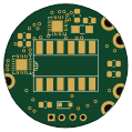 TI MSP430/CC
Elektronika-1
BenjaminSoelberg
29.5 × 29.5 mm14 parts4LGPL-3.029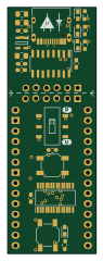 TI MSP430/CC
CheeseDip
upsidedownlabs
21.6 × 60 mm27 parts2LCERN-OHL-S-2.021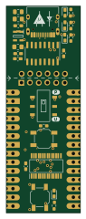 TI MSP430/CC
CheeseDip-Castellated
21.6 × 60 mm27 parts2LCERN-OHL-S-2.021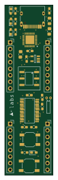 TI MSP430/CC
MSP430 Breadstick - Apple Sauce
18.5 × 65.8 mm31 parts2LCERN-OHL-S-2.021