
Kyps75 keeb

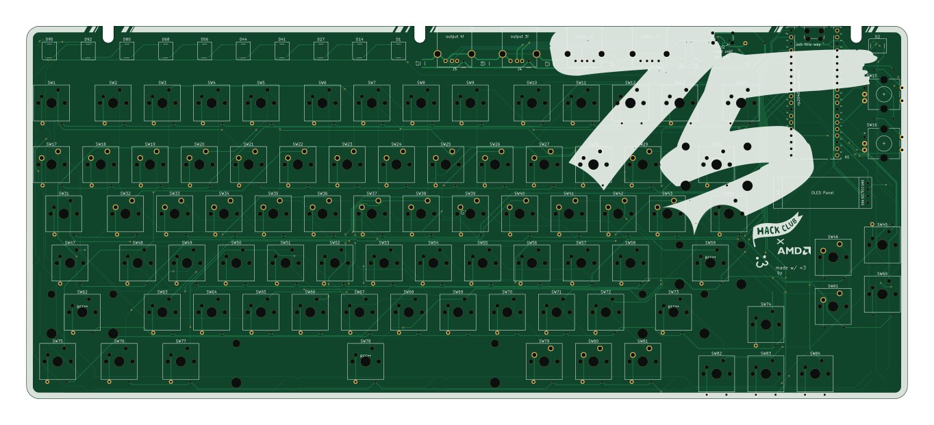
About the Kyps75 keeb PCB
Kyps75 keeb is an open source RP2040/RP2350 PCB design by theonlydesigner, published on GitHub. It is a 2-layer board measuring 340.5 × 144 mm, with 206 components from 10 distinct parts.
Its main chip is the RaspberryPi_Pico, from the RP2040/RP2350 family. Other key parts include the SL2.1A. By type, the board carries 107 diodes, 84 switches, 7 capacitors, 5 connectors, 2 ICs and 1 module.
It belongs with the keyboards and displays & leds designs in this gallery.
From the project
welcome to the KYPS75 repository. this is a scratch-built 75% mechanical keyboard featuring dual rotary encoders and an OLED display [because why have one knob when you can have two?]. i originally designed this after realizing my 60% board was actively sabotaging my daily workfl
welcome to the KYPS75 repository. this is a scratch-built 75% mechanical keyboard featuring dual rotary encoders and an OLED display [because why have one knob when you can have two?]. i originally designed this after realizing my 60% board was actively sabotaging my daily workflow [turns out arrow keys are actually useful, who knew].
1. PCB SMT Component Soldering: Solder all surface-mount components (diodes, resistors, capacitors, OLED headers, rotary encoder pins, and controller MCU/sockets) onto the custom PCB. 2. Switch Placement & Soldering: Push mechanical switches into the top plate…
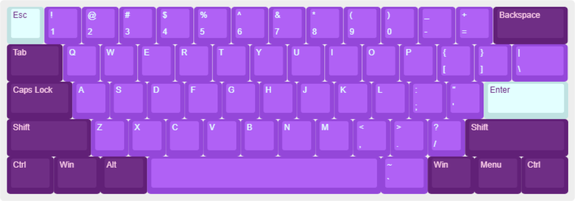
Main components on the Kyps75 keeb
Kyps75 keeb bill of materials (BOM)
206 components, 10 distinct parts.
| Qty | Part | Footprint | Refs |
|---|---|---|---|
| 1 | ~ | SSD1306-0.91-OLED-4pin-128x32 | U1 |
| 1 | SL2.1A | SOIC-16_4.55x10.3mm_P1.27mm | U2 |
| 1 | RaspberryPi_Pico | RaspberryPi_Pico_Common_Unspecified | A1 |
| 4 | USB_A | USB_A_Molex_67643_Horizontal | J1, J3, J4, J5 |
| 1 | USB_B_Micro | USB_Micro-B_Wuerth_629105150521 | J2 |
| 82 | Keyswitch | SW_Cherry_MX_1.00u_PCB | SW1, SW2, SW3, SW4, SW5, SW6, SW7, SW8 +74 |
| 2 | RotaryEncoder_Switch | RotaryEncoder_Alps_EC11E-Switch_Vertical_H20mm | SW15, SW16 |
| 22 | SK6812 | LED_SK6812_PLCC4_5.0x5.0mm_P3.2mm | D1, D2, D14, D15, D27, D28, D41, D42 +14 |
| 85 | D | D_DO-35_SOD27_P7.62mm_Horizontal | D4, D5, D6, D7, D8, D9, D10, D11 +77 |
| 7 | C | C_1206_3216Metric_Pad1.33x1.80mm_HandSolder | C1, C2, C3, C4, C5, C6, C7 |
Kyps75 keeb design files
The KiCad project lives in the theonlydesigner/kyps75_keeb repository on GitHub; these links point at the commit this page was built from.
- LayoutPCB/kyps75.kicad_pcb
- SchematicPCB/kyps75.kicad_sch
Kyps75 keeb: common questions
What microcontroller does the Kyps75 keeb use?
The Kyps75 keeb is built around the RaspberryPi_Pico, from the RP2040/RP2350 family.
How big is the Kyps75 keeb PCB?
The Kyps75 keeb measures 340.5 × 144 mm, has 2 copper layers and is 1.6 mm thick.
How many components are on the Kyps75 keeb?
206 components, from 10 distinct parts. The full bill of materials is listed on this page.
Where can I download the Kyps75 keeb design files?
From the theonlydesigner/kyps75_keeb repository on GitHub, which has the KiCad layout and the schematic; the links under Design files point to each one.
Can I use the Kyps75 keeb design in my own project?
The repository has no license, so all rights stay with theonlydesigner. Use it as a reference, and ask the author before reusing the design.
Can I test firmware for the Kyps75 keeb without the hardware?
Yes. HardLabs builds a simulation of the board from its netlist and BOM, so you can run and debug RP2040/RP2350 firmware against it before you order a PCB.
Similar boards
 RP2040/RP2350
OSO-BOOK-C1
joeycastillo
85 × 115 mm29 parts2LCC-BY-SA-4.08.1k RP2040/RP2350
Corne chocolate
foostan
277.2 × 107.5 mm164 parts2LCC-BY-4.07.7k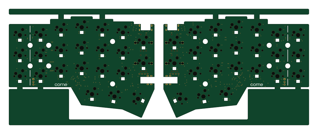 RP2040/RP2350
Corne cherry
277.2 × 107.5 mm164 parts2LCC-BY-4.07.7k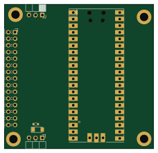 RP2040/RP2350
LogicAnalyzer
gusmanb
57 × 55.2 mm6 parts2LGPL-3.05.0k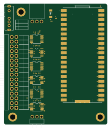 RP2040/RP2350
Jitx design
55.5 × 65 mm26 parts4LGPL-3.05.0k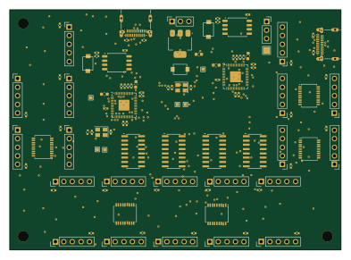 RP2040/RP2350
Main
google
98 × 71 mm102 parts2LApache-2.02.9k