
Arm jtag20 dip

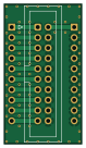
About the Arm jtag20 dip PCB
Arm jtag20 dip is an open source PCB design by tnishinaga, published on GitHub. It is a 2-layer board measuring 18.9 × 34.1 mm, with 3 components from 2 distinct parts.
It belongs with the usb & debug tools designs in this gallery.
Arm jtag20 dip bill of materials (BOM)
3 components, 2 distinct parts — part numbers from the project's BOM.
| Qty | Part | Footprint | Refs |
|---|---|---|---|
| 2 | Conn_01x10_Male | PinHeader_1x10_P2.54mm_Vertical | J1, J2 |
| 1 | Conn_ARM_JTAG_SWD_20 | IDC-Header_2x10_P2.54mm_Vertical | J3 |
Arm jtag20 dip design files
The KiCad project lives in the tnishinaga/seccamp2022_pcb repository on GitHub; these links point at the commit this page was built from.
Arm jtag20 dip: common questions
How big is the Arm jtag20 dip PCB?
The Arm jtag20 dip measures 18.9 × 34.1 mm, has 2 copper layers and is 1.6 mm thick.
How many components are on the Arm jtag20 dip?
3 components, from 2 distinct parts, with part numbers taken from the project's own BOM. The full bill of materials is listed on this page.
Where can I download the Arm jtag20 dip design files?
From the tnishinaga/seccamp2022_pcb repository on GitHub, which has the KiCad layout and the BOM; the links under Design files point to each one.
Can I use the Arm jtag20 dip design in my own project?
The repository has no license, so all rights stay with tnishinaga. Use it as a reference, and ask the author before reusing the design.
More boards in seccamp2022_pcb
Similar boards
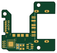
FW-EC-DongleHiderPlus
LeoDJ
28.2 × 26.1 mm14 parts4LCERN-OHL-W-2.0490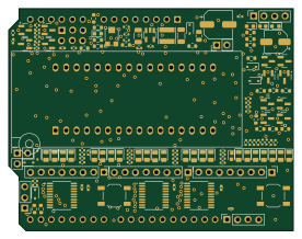
Relatively-Universal-ROM-Programmer
AndersBNielsen
68.8 × 53.6 mm141 parts2LGPL-3.0253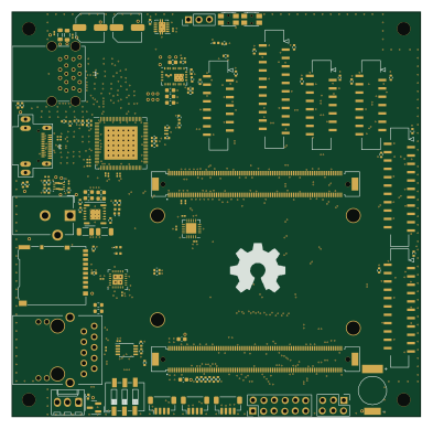
Ovc5
osrf
98 × 97 mm197 parts6LApache-2.0208
Easy pdk programmer hardware
free-pdk
26.7 × 21.6 mm28 parts2LCC-BY-SA-4.0206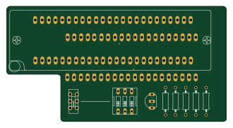
27c160-tl866-adapter
mafe72
82.4 × 43.1 mm10 partsGPL-3.0147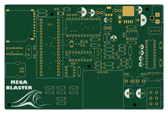
STM32 VGM Player YM2612 SN76489
AidanHockey5
138.4 × 91.4 mm84 parts2LAGPL-3.0117