
PS2 Debug Probe

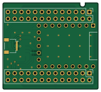
About the PS2 Debug Probe PCB
PS2 Debug Probe is an open source RP2040/RP2350 PCB design by tschicki, published on GitHub under the MIT license. It is a 2-layer board measuring 35.6 × 32.2 mm, with 4 components from 4 distinct parts.
Its main chip is the RP2040-ZERO, from the RP2040/RP2350 family. By type, the board carries 2 ICs and 2 connectors.
From the project
A custom designed PS2 Portable
This directory contains all the PCB projects. You will find the Gerber files in the respective Gerber/ folders. The BOM is in ibom format and can be found in the BOM/ folders where applicable. For very simple PCBs like the gamepad flex PCBs you will find the needed components in Part 5 of the project documentation.
If you need the BOM in CSV format, you can open the ibom files and export the content as CSV.
Main components on the PS2 Debug Probe
PS2 Debug Probe bill of materials (BOM)
4 components, 4 distinct parts — part numbers from the project's BOM.
| Qty | Part | Footprint | Refs |
|---|---|---|---|
| 1 | RP2040-ZERO | MODULE_RP2040-ZERO | U1 |
| 1 | ~ | FT2232H_mini_module_jtag | U2 |
| 1 | FTSH-107-01-F-DV-K-P-TR Debug | FTSH-107-01-F-DV-K-P-TR | J1 |
| 1 | SM03B-SRSS-TB DEBUG_SWD | JST_SM03B-SRSS-TB(LF)(SN) | J101 |
PS2 Debug Probe design files
The KiCad project lives in the tschicki/PS2-Portable repository on GitHub; these links point at the commit this page was built from.
PS2 Debug Probe: common questions
What microcontroller does the PS2 Debug Probe use?
The PS2 Debug Probe is built around the RP2040-ZERO, from the RP2040/RP2350 family.
How big is the PS2 Debug Probe PCB?
The PS2 Debug Probe measures 35.6 × 32.2 mm, has 2 copper layers and is 1.6 mm thick.
How many components are on the PS2 Debug Probe?
4 components, from 4 distinct parts, with part numbers taken from the project's own BOM. The full bill of materials is listed on this page.
Where can I download the PS2 Debug Probe design files?
From the tschicki/PS2-Portable repository on GitHub, which has the KiCad layout, the schematic and the BOM; the links under Design files point to each one.
Can I use the PS2 Debug Probe design in my own project?
Yes, under the terms of its MIT license, which tschicki chose for the repository.
Can I test firmware for the PS2 Debug Probe without the hardware?
Yes. HardLabs builds a simulation of the board from its netlist and BOM, so you can run and debug RP2040/RP2350 firmware against it before you order a PCB.
More boards in PS2-Portable
 RP2040/RP2350
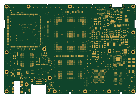
PS2 AIO Mainboard
121 × 83 mm568 parts6LMIT202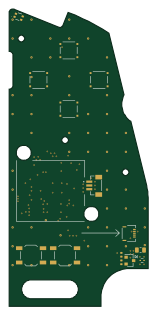 RP2040/RP2350
Gamepad Right
36.8 × 78.7 mm42 parts4LMIT202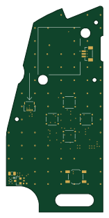 RP2040/RP2350
Gamepad Left
36.8 × 78.7 mm34 parts4LMIT202 RP2040/RP2350
Rp2040-memcard
24 × 32 mm28 parts2LMIT202
Memory Card
24 × 32 mm17 parts2LMIT202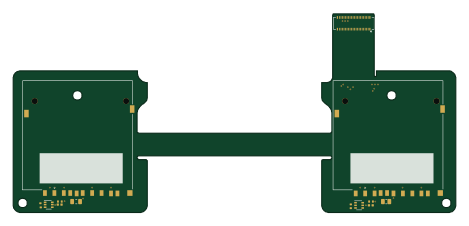
PS2 memcard flex
117.2 × 52.6 mm13 parts2LMIT202
PS2 Reballing Stencils Eval
190 × 190 mm9 parts2LMIT202
Flex L1 L2
14.7 × 20.6 mm3 parts2LMIT202
Flex R1 R2
14.7 × 20.6 mm3 parts2LMIT202
Similar boards
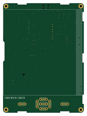 RP2040/RP2350
Open Book Abridged Edition
joeycastillo
85 × 115 mm29 parts2LCC-BY-SA-4.08.1k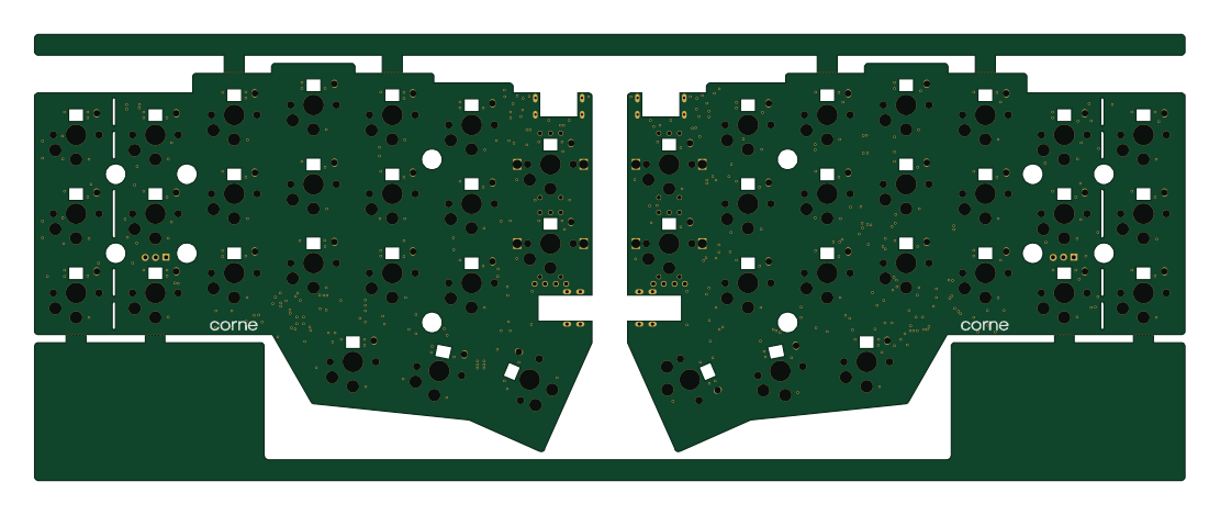 RP2040/RP2350
Corne
foostan
277.2 × 107.5 mm164 parts2LCC-BY-4.07.7k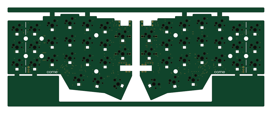 RP2040/RP2350
Corne
277.2 × 107.5 mm164 parts2LCC-BY-4.07.7k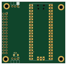 RP2040/RP2350
LogicAnalyzer
gusmanb
57 × 55.2 mm6 parts2LGPL-3.05.0k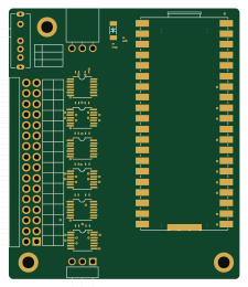 RP2040/RP2350
Jitx design
55.5 × 65 mm26 parts4LGPL-3.05.0k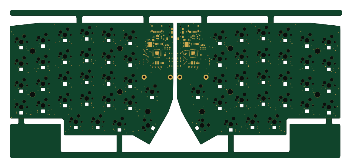 RP2040/RP2350
Pro V2
kata0510
290.1 × 130 mm270 parts2LMIT2.3k