
Pcb design

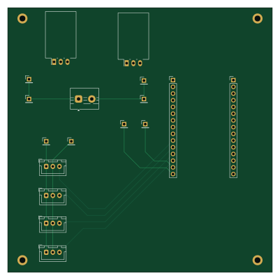
About the Pcb design
Pcb design is an open source PCB design by TuksBaja-Electrical-Subteam, published on GitHub. It is a 2-layer board measuring 100 × 100 mm, with 15 components from 4 distinct parts.
It belongs with the power & battery and sensors designs in this gallery.
From the project
KiCAD wiring schematics (schematics and PCB layouts) for our vehicle's electronics
Hardware design files for the TuksBaja SAE Baja vehicle telemetry system (iteration 1).
The board takes the vehicle's 12V battery, steps it down to 5V, and hosts an ESP32 dev board that reads four A3144 hall effect wheel-speed sensors and drives a steering-wheel display.
Firmware lives in a separate repo: esp32-code
Key design decisions: - ESP32 dev board socketed on female headers — not a bare module — so the proven USB/flash/regulator circuitry stays off our board and a damaged dev board can be swapped in seconds. - Buck converter design generated with TI WEBENCH (see reference/) and…
Pcb design bill of materials (BOM)
15 components, 4 distinct parts.
| Qty | Part | Footprint | Refs |
|---|---|---|---|
| 1 | Screw_Terminal_01x02 | TerminalBlock_MaiXu_MX126-5.0-02P_1x02_P5.00mm | Battery_Terminal1 |
| 2 | Conn_01x15 | PinHeader_1x15_P2.54mm_Vertical | ESP_LEFT1, ESP_RIGHT1 |
| 4 | Conn_01x03 | JST_XH_B3B-XH-A_1x03_P2.50mm_Vertical | FL_WS1, FR_WS1, RL_WS1, RR_WS1 |
| 8 | Conn_01x01_Pin | PinHeader_1x01_P2.54mm_Vertical | IN_GND1, IN_GND2, OUT_GND1, OUT_GND2, VIN1, VIN2, VOUT1, VOUT2 |
Pcb design design files
The KiCad project lives in the TuksBaja-Electrical-Subteam/pcb-design repository on GitHub; these links point at the commit this page was built from.
Pcb design: common questions
How big is the Pcb design?
The Pcb design measures 100 × 100 mm, has 2 copper layers and is 1.6 mm thick.
How many components are on the Pcb design?
15 components, from 4 distinct parts. The full bill of materials is listed on this page.
Where can I download the Pcb design design files?
From the TuksBaja-Electrical-Subteam/pcb-design repository on GitHub, which has the KiCad layout and the schematic; the links under Design files point to each one.
Can I use the Pcb design design in my own project?
The repository has no license, so all rights stay with TuksBaja-Electrical-Subteam. Use it as a reference, and ask the author before reusing the design.
Similar boards
Sensor smd
scottbez1
40 × 20 mm5 parts2LApache-2.04.2k
Sensors
StuckAtPrototype
15.2 × 9 mm14 parts4LApache-2.03.8k
EinkPDA screen
TalismanDesign
95 × 54 mm27 parts2LApache-2.02.0k
Stack chan
stack-chan
50 × 50 mm33 parts2LApache-2.01.7k
Display Carrier
AxxAxx
35.6 × 58.2 mm5 parts2LGPL-3.01.7k
Microphone
Mentra-Community
5.5 × 6.1 mm6 parts2LMIT1.2k