
Main-GPSSwitching

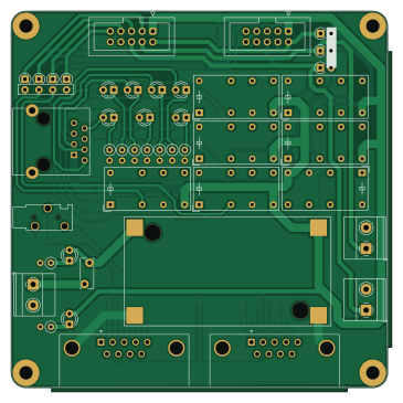
About the Main-GPSSwitching PCB
Main-GPSSwitching is an open source PCB design by twfth9, published on GitHub under the GPL-3.0 license. It is a 2-layer board measuring 91 × 91 mm, with 72 components from 16 distinct parts.
Other key parts include the 12V Variable Boost Buck Converter. By type, the board carries 27 jumpers, 16 diodes, 9 resistors, 7 connectors, 7 relays and 1 IC.
Main components on the Main-GPSSwitching
Main-GPSSwitching bill of materials (BOM)
72 components, 16 distinct parts.
| Qty | Part | Footprint | Refs |
|---|---|---|---|
| 1 | 12V Variable Boost Buck Converter | BoostBuck | U101 |
| 1 | 2x05 IDC Header - OUT 1 | IDC-Header_2x05_P2.54mm_Vertical | J102 |
| 1 | Selector Knob Connector | Mystery_RJ45 | J103 |
| 1 | External Relay Enable | TerminalBlock_Phoenix_MKDS-1,5-2_1x02_P5.00mm_Horizontal | J104 |
| 1 | KrakenSDR Relay Enable | TerminalBlock_Phoenix_MKDS-1,5-2_1x02_P5.00mm_Horizontal | J107 |
| 1 | 2x05 IDC Header - OUT 2 | IDC-Header_2x05_P2.54mm_Vertical | J108 |
| 1 | D-700 GPS | Mystery_3.5mm | J111 |
| 1 | Power IN | TerminalBlock_Phoenix_MKDS-1,5-2_1x02_P5.00mm_Horizontal | J112 |
| 1 | 1A Trip | Fuse_Bourns_MF-RG300 | F101 |
| 4 | Mounting Hole | M3_Mounting | H101, H102, H103, H104 |
| 25 | Jumper_2_Bridged | 1.0mm_Bridge | JP101, JP102, JP103, JP104, JP105, JP106, JP107, JP108 +17 |
| 2 | Jumper_2_Bridged | 1.0mm_Bridge_Open | JP114, JP118 |
| 7 | FINDER-40.52 | Relay_DPDT_Finder_30.22 | K101, K102, K103, K104, K105, K106, K107 |
| 7 | D_Small_Filled | D_A-405_P2.54mm_Vertical_AnodeUp | D101, D102, D103, D104, D105, D106, D107 |
| 9 | LED | LED_D3.0mm | D108, D109, D110, D111, D112, D113, D114, D115 +1 |
| 9 | 680Ω | R_Axial_DIN0207_L6.3mm_D2.5mm_P2.54mm_Vertical | R101, R102, R103, R104, R105, R106, R107, R108 +1 |
Main-GPSSwitching design files
The KiCad project lives in the twfth9/Kenwood-Handset-Switch-PCB repository on GitHub; these links point at the commit this page was built from.
Main-GPSSwitching: common questions
How big is the Main-GPSSwitching PCB?
The Main-GPSSwitching measures 91 × 91 mm, has 2 copper layers and is 1.6 mm thick.
How many components are on the Main-GPSSwitching?
72 components, from 16 distinct parts. The full bill of materials is listed on this page.
Where can I download the Main-GPSSwitching design files?
From the twfth9/Kenwood-Handset-Switch-PCB repository on GitHub, which has the KiCad layout and the schematic; the links under Design files point to each one.
Can I use the Main-GPSSwitching design in my own project?
Yes, under the terms of its GPL-3.0 license, which twfth9 chose for the repository.
More boards in Kenwood-Handset-Switch-PCB
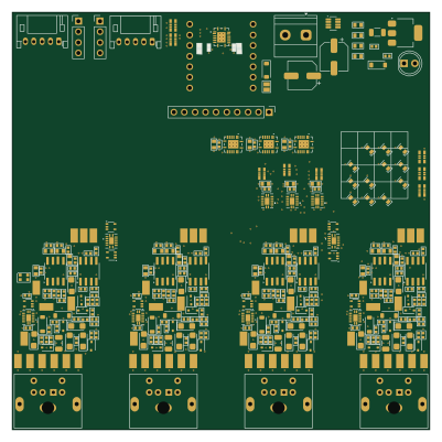 Microchip SAM
DATA Switcher
100 × 100 mm667 parts4LGPL-3.00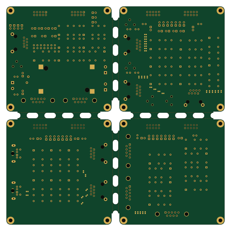
InterfaceModule
187 × 187 mm243 parts2LGPL-3.00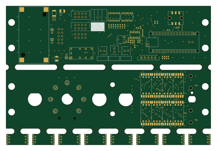
1-DIN Control Panel
177.8 × 120.9 mm82 parts2LGPL-3.00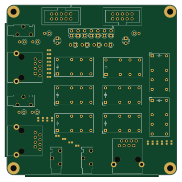
MicSwitch
91 × 91 mm63 parts2LGPL-3.00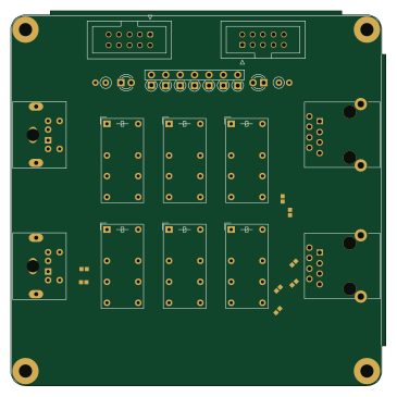
DataSwitching
91 × 91 mm55 parts2LGPL-3.00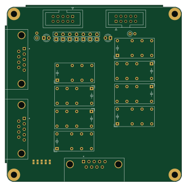
COMSwitching
91 × 91 mm52 parts2LGPL-3.00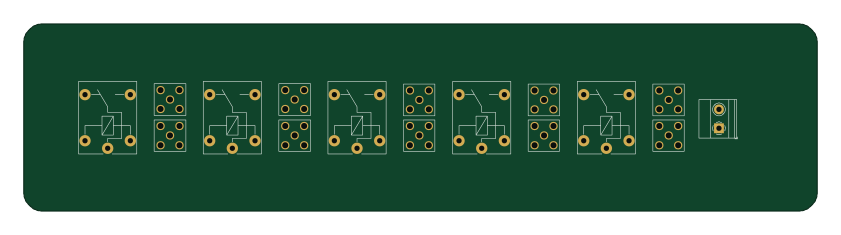
KrakenSDR AntDisconnect ThruThin
210 × 49.5 mm16 parts2LGPL-3.00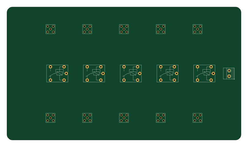
KrakenSDR AntDisconnect Thru
210 × 119.9 mm16 parts2LGPL-3.00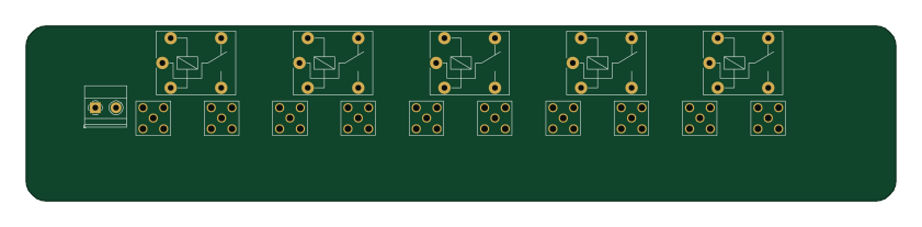
KrakenSDR AntDisconnect Edge
210 × 42.2 mm16 parts2LGPL-3.00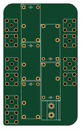
5Pole RF Toggle
40 × 65.9 mm16 parts2LGPL-3.00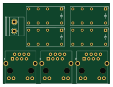
KenwoodHandsetSwitch
57.6 × 43.5 mm8 parts2LGPL-3.00