UPD-board

About the UPD-board
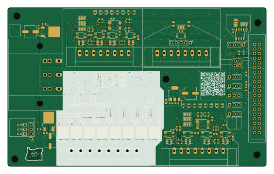
UPD-board is an open source PCB design by uniclogs, published on GitHub under the GPL-3.0 license. It is a 2-layer board measuring 140.7 × 86.5 mm, with 184 components from 33 distinct parts.
Other key parts include the MAX7310ATE+T, ADT7410TRZ, ADS1115IDGS, UA78M33 and U_RasPi_40pin. By type, the board carries 46 resistors, 28 capacitors, 27 diodes, 24 jumpers, 22 transistors and 15 ICs.
From the project
University Class Open Ground Station Hardware
This board controls all of the switching of power to components in the ground station. It accepts it's commands through an I2C interface on the Stationd computer.
The switching is acomplished through 3 I2C GPIO device setup as 24 output bits. The bits control mosfet switches provideing both 5VDC and 12VDC circuits.
The board also has an A/D to monitor the RF Power Amplifiers output power detectors. The characteristics of this power measurement is detailed in the power amplifier testing spreadsheet unfer RF-systems.
Main components on the UPD-board
UPD-board bill of materials (BOM)
184 components, 33 distinct parts — part numbers from the project's BOM.
| Qty | Part | Footprint | Refs |
|---|---|---|---|
| 3 | MAX7310ATE+T MAX7310 | TSSOP-16_4.4x5mm_P0.65mm | U1, U2, U3 |
| 1 | ADT7410TRZ | SOIC-8_3.9x4.9mm_P1.27mm | U4 |
| 1 | ADS1115IDGS | TSSOP-10_3x3mm_P0.5mm | U5 |
| 1 | UA78M33 | SOT-223-3_TabPin2 | U6 |
| 1 | U_RasPi_40pin | IDC-Header_2x20_P2.54mm_Vertical | U7 |
| 8 | TC4427 | MSOP-8_3x3mm_P0.65mm | U8, U9, U10, U11, U12, U13, U14, U15 |
| 12 | DMN61D8L-LVT | TSOT26-6 | Q1, Q4, Q7, Q10, Q13, Q14, Q15, Q16 +4 |
| 10 | SUD50P08-25L-E3 | TO-252-3_TabIsPin2 | Q2, Q3, Q5, Q6, Q8, Q9, Q11, Q12 +2 |
| 2 | Conn_01x04 | PinHeader_1x04_P2.54mm_Vertical | J1, J14 |
| 5 | Conn_01x03 | PinHeader_1x03_P2.54mm_Vertical | J2, J3, J4, J5, J6 |
| 1 | PI 1924143 | J_PhoenixContact_MC_1,5_8-GF-5.08_1x08_P5.08mm_Horizontal_ThreadedFlange | J7 |
| 1 | PI 1827923 | PhoenixContact_MC_1,5_8-GF-3.81_1x08_P3.81mm_Horizontal_ThreadedFlange | J8 |
| 2 | PI 1827486 | J_PhoenixContact_MC_1,5_8-GF-3.81_1x08_P3.81mm_45degree_ThreadedFlange | J9, J10 |
| 1 | PC 1720806 | PhoenixContact_GMSTBA_2,5_3-G-7,62_1x03_P7.62mm_Horizontal | J11 |
| 1 | Conn_02x02_Odd_Even | PinHeader_2x02_P2.54mm_Vertical | J12 |
| 1 | Conn_01x05 | PinHeader_1x05_P2.54mm_Vertical | J13 |
| 5 | MountingHole | H-MCMASTER-94100A150 | H1, H2, H3, H4, H5 |
| 12 | SolderJumper3 | SolderJumper-3_P1.3mm_Bridged12_Pad1.0x1.5mm | JP1, JP2, JP3, JP4, JP5, JP6, JP7, JP8 +4 |
| 8 | SolderJumper | SolderJumper-2_P1.3mm_Open_RoundedPad1.0x1.5mm | JP14, JP15, JP18, JP19, JP22, JP23, JP26, JP27 |
| 4 | SolderJumper-HP | JP-SOLDER-2way-HP | JP24, JP25, JP28, JP29 |
Show 13 more
| Qty | Part | Footprint | Refs |
|---|---|---|---|
| 3 | PWR | LED_0603_1608Metric | D1, D2, D3 |
| 24 | LED | LED_0603_1608Metric | D4, D5, D6, D7, D8, D9, D10, D11 +16 |
| 2 | WLBD2012HCU310TH FerriteBead | C_0805_2012Metric | FB1, FB3 |
| 1 | Link | R_0805_2012Metric | FB2 |
| 17 | CL10B104KB8NNWC 0.1uf | C_0603_1608Metric | C1, C2, C3, C4, C5, C6, C7, C8 +9 |
| 3 | 865080445010 100u | CP_Elec_6.3x5.9 | C10, C11, C20 |
| 8 | CL10B105KA8NNNC 1u | C_0603_1608Metric | C12, C13, C14, C15, C16, C17, C18, C19 |
| 7 | 4k7 | R_0603_1608Metric | R1, R2, R3, R4, R5, R27, R28 |
| 2 | 1500 | R_0603_1608Metric | R6, R8 |
| 1 | 620 | R_0603_1608Metric | R7 |
| 10 | 10k | R_0603_1608Metric | R9, R11, R13, R15, R17, R19, R21, R23 +2 |
| 8 | gate | R_0603_1608Metric | R10, R12, R14, R16, R18, R20, R22, R26 |
| 18 | RAVF164DJT10K0 10k | R_Array_Convex_4x0603 | RN1, RN2, RN3, RN4, RN5, RN6, RN7, RN8 +10 |
UPD-board design files
The KiCad project lives in the uniclogs/uniclogs-hardware repository on GitHub; these links point at the commit this page was built from.
UPD-board: common questions
How big is the UPD-board?
The UPD-board measures 140.7 × 86.5 mm, has 2 copper layers and is 1.6 mm thick.
How many components are on the UPD-board?
184 components, from 33 distinct parts, with part numbers taken from the project's own BOM. The full bill of materials is listed on this page.
Where can I download the UPD-board design files?
From the uniclogs/uniclogs-hardware repository on GitHub, which has the KiCad layout, the schematic and the BOM; the links under Design files point to each one.
Can I use the UPD-board design in my own project?
Yes, under the terms of its GPL-3.0 license, which uniclogs chose for the repository.