
F103 V2

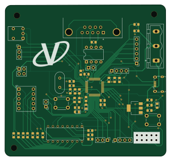
About the F103 V2 PCB
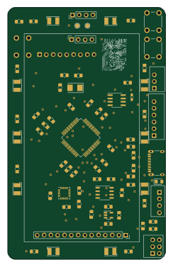
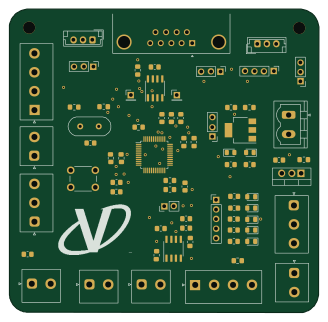
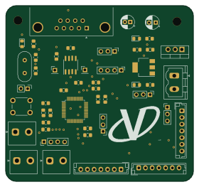
F103 V2 is an open source STM32 PCB design by Vaaarad07, published on GitHub under the MIT license. It is a 2-layer board measuring 84.4 × 79.2 mm, with 55 components from 25 distinct parts.
Its main chip is the STM32F103C8Tx, from the STM32 family. Other key parts include the AMS1117-3.3, 74LS47, SA39-12EWA and MCP2551-I-SN. By type, the board carries 20 resistors, 12 capacitors, 11 connectors, 5 ICs, 3 switches and 3 diodes.
It belongs with the usb & debug tools designs in this gallery.
From the project
A repo with STM32 based PCB designs
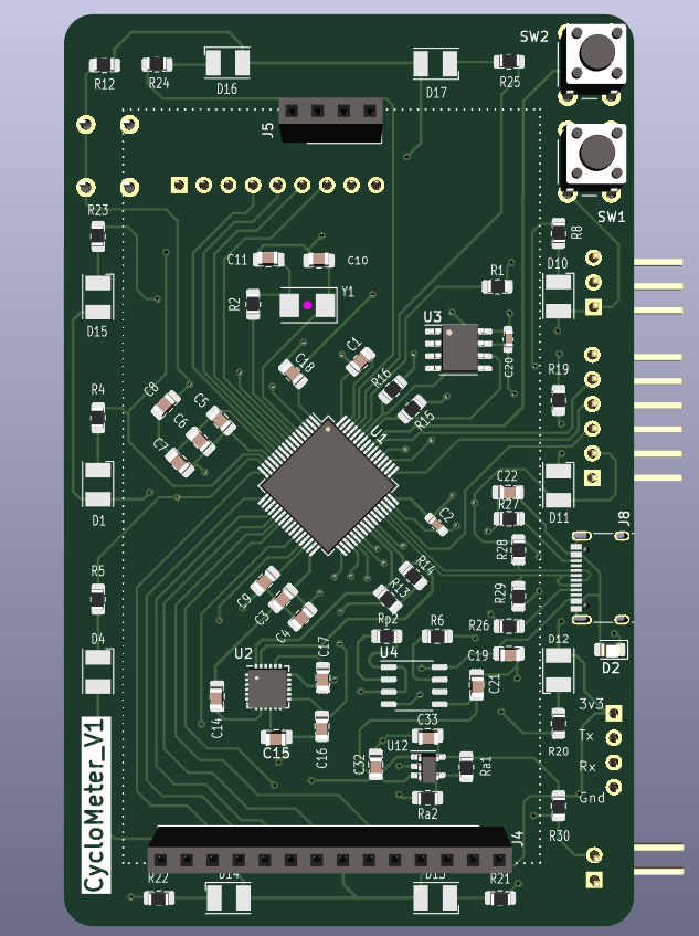
Main components on the F103 V2
F103 V2 bill of materials (BOM)
55 components, 25 distinct parts.
| Qty | Part | Footprint | Refs |
|---|---|---|---|
| 1 | AMS1117-3.3 | SOT-223-3_TabPin2 | U1 |
| 1 | 74LS47 | DIP794W45P254L1930H508Q16 | U2 |
| 1 | SA39-12EWA | Sx39-1xxxxx | U3 |
| 1 | STM32F103C8Tx | LQFP-48_7x7mm_P0.5mm | U4 |
| 1 | MCP2551-I-SN | DIP-8_W7.62mm | U5 |
| 1 | Crystal | Crystal_HC49-U_Vertical | Y1 |
| 2 | Conn_01x04_Male | PinHeader_1x04_P2.54mm_Vertical | J1, J8 |
| 2 | Conn_01x03_Male | PinHeader_1x03_P2.54mm_Vertical | J2, J5 |
| 1 | Conn_01x06_Male | PinHeader_1x06_P2.54mm_Vertical | J3 |
| 1 | Conn_02x02_Odd_Even | PinHeader_2x02_P2.54mm_Vertical | J4 |
| 2 | Conn_01x02_Male | PinHeader_1x02_P2.54mm_Vertical | J6, J12 |
| 1 | Conn_02x05_Top_Bottom | PinSocket_2x05_P2.54mm_Vertical | J7 |
| 1 | USB_B_Micro | USB_Micro-B_Wuerth_629105150521 | J9 |
| 1 | Conn_01x03_Male | PhoenixContact_GMSTBVA_2,5_3-G-7,62_1x03_P7.62mm_Vertical | J11 |
| 2 | SW_Push | SW_PUSH_6mm_H5mm | SW1, SW3 |
| 1 | SW_SPDT | SW_Push_1P2T_Vertical_E-Switch_800UDP8P1A1M6 | SW2 |
| 3 | LED | LED_0805_2012Metric_Pad1.15x1.40mm_HandSolder | D1, D2, D3 |
| 7 | 100nF | C_0805_2012Metric_Pad1.18x1.45mm_HandSolder | C1, C6, C7, C8, C9, C10, C11 |
| 2 | 22uF | C_0805_2012Metric_Pad1.18x1.45mm_HandSolder | C2, C4 |
| 2 | 30pF | C_0805_2012Metric_Pad1.18x1.45mm_HandSolder | C3, C5 |
Show 5 more
| Qty | Part | Footprint | Refs |
|---|---|---|---|
| 1 | 1uF | C_0805_2012Metric_Pad1.18x1.45mm_HandSolder | C12 |
| 12 | R_US | R_0805_2012Metric_Pad1.20x1.40mm_HandSolder | R1, R2, R3, R8, R9, R10, R11, R12 +4 |
| 3 | 10k | R_0805_2012Metric_Pad1.20x1.40mm_HandSolder | R4, R5, R7 |
| 4 | 1.5k | R_0805_2012Metric_Pad1.20x1.40mm_HandSolder | R6, R15, R17, R18 |
| 1 | 120 | R_0805_2012Metric_Pad1.20x1.40mm_HandSolder | R16 |
F103 V2 design files
The KiCad project lives in the Vaaarad07/PCB_Designs repository on GitHub; these links point at the commit this page was built from.
F103 V2: common questions
What microcontroller does the F103 V2 use?
The F103 V2 is built around the STM32F103C8Tx, from the STM32 family.
How big is the F103 V2 PCB?
The F103 V2 measures 84.4 × 79.2 mm, has 2 copper layers and is 1.6 mm thick.
How many components are on the F103 V2?
55 components, from 25 distinct parts. The full bill of materials is listed on this page.
Where can I download the F103 V2 design files?
From the Vaaarad07/PCB_Designs repository on GitHub, which has the KiCad layout and the schematic; the links under Design files point to each one.
Can I use the F103 V2 design in my own project?
Yes, under the terms of its MIT license, which Vaaarad07 chose for the repository.
Can I test firmware for the F103 V2 without the hardware?
Yes. HardLabs builds a simulation of the board from its netlist and BOM, so you can run and debug STM32 firmware against it before you order a PCB.
More boards in PCB_Designs
Similar boards
 STM32
STM32LumenPnP Motherboard
opulo-inc
149 × 95 mm296 parts4LCC-BY-SA-4.03.7k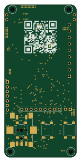 STM32
STM32AxxSolder
AxxAxx
39 × 82.5 mm122 parts2LGPL-3.01.7k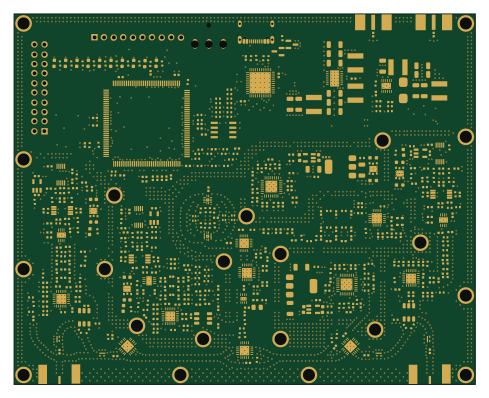 STM32
STM32LibreVNA
jankae
122 × 98 mm592 parts6LGPL-3.01.6k STM32
STM32AIOC
skuep
21 × 31.5 mm47 parts2LMIT1.4k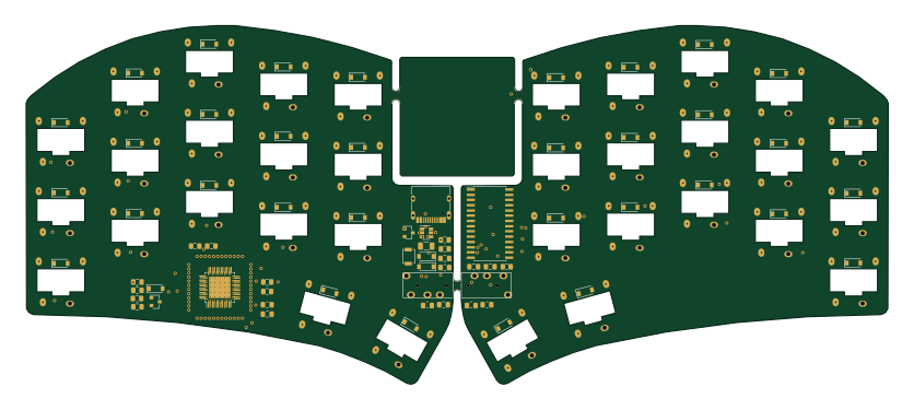 STM32
STM32Ferris
pierrechevalier83
208.8 × 86.8 mm102 parts2LSHL-2.11.3k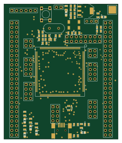 STM32
STM32176 pin board
rusefi
61.8 × 73.2 mm76 parts2LGPL-3.01.2k