
Stencil

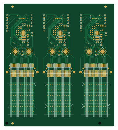
About the Stencil PCB
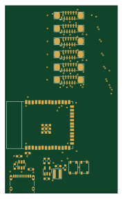
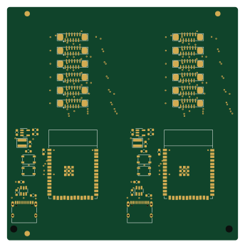
Stencil is an open source PCB design by wselsbe, published on GitHub. It is a 2-layer board measuring 95 × 105.2 mm, with 36 components from 17 distinct parts.
Other key parts include the HV509 and DRV2665. By type, the board carries 15 test points, 8 capacitors, 5 resistors, 3 ICs, 2 connectors and 1 diode.
It belongs with the displays & leds designs in this gallery.
From the project
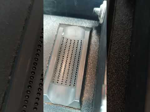
This project aims to recreate the Optacon (OPtical to TActile CONverter), a reading aid for the blind. The user moves a small camera module over a document to scan one letter at a time. The main module has a "tactile display": a 6x24 array of vibrating pins, so the user can feel
This project aims to recreate the Optacon (OPtical to TActile CONverter), a reading aid for the blind. The user moves a small camera module over a document to scan one letter at a time. The main module has a "tactile display": a 6x24 array of vibrating pins, so the user can feel the shape of the letter being scanned with their fingertip.
The vibrating pins are actuated by piezoelectric bimorphs, similar to those used in refreshable braille displays. The Optacon uses vibrating pins instead of static, and achieves a higher pin density: 1mm x 2mm versus 2.5mm x 2.5mm. The following videos show…
Main components on the Stencil
Stencil bill of materials (BOM)
36 components, 17 distinct parts.
| Qty | Part | Footprint | Refs |
|---|---|---|---|
| 2 | HV509 | HVQFN-32-1EP_5x5mm_P0.5mm_EP3.1x3.1mm_ThermalVias | U1, U2 |
| 1 | DRV2665 | Texas_S-PVQFN-N20_EP2.7x2.7mm_ThermalVias | U3 |
| 1 | Conn_01x12 | Hirose_FH34SRJ-12S-0.5SH | J1 |
| 1 | Conn_01x40_Socket | Hirose_FH34SRJ-40S-0.5SH | J2 |
| 2 | VDD | TestPoint_THTPad_D1.0mm_Drill0.5mm | TP1, TP15 |
| 1 | TestPoint | TestPoint_THTPad_1.0x1.0mm_Drill0.5mm | TP2 |
| 12 | TestPoint | TestPoint_THTPad_D1.0mm_Drill0.5mm | TP3, TP4, TP5, TP6, TP7, TP8, TP9, TP10 +4 |
| 1 | Conn_01x22 | piezox20 | piezo1 |
| 1 | D | D_SOD-123F | D1 |
| 1 | 3.3 µH | TDK_VLS_3012 | L1 |
| 3 | 1 µF | C_0603_1608Metric | C1, C6, C7 |
| 3 | 0.1 µF | C_0603_1608Metric | C2, C3, C8 |
| 1 | 0.1 µF 150V+ | C_0805_2012Metric | C4 |
| 1 | 10 µF | C_0603_1608Metric | C5 |
| 1 | 549k | R_0603_1608Metric | R1 |
| 2 | 6.98k | R_0603_1608Metric | R2, R3 |
| 2 | 3.3k | R_0603_1608Metric | R4, R5 |
Stencil design files
The KiCad project lives in the wselsbe/optacon repository on GitHub; these links point at the commit this page was built from.
Stencil: common questions
How big is the Stencil PCB?
The Stencil measures 95 × 105.2 mm, has 2 copper layers and is 1.6 mm thick.
How many components are on the Stencil?
36 components, from 17 distinct parts. The full bill of materials is listed on this page.
Where can I download the Stencil design files?
From the wselsbe/optacon repository on GitHub, which has the KiCad layout; the links under Design files point to each one.
Can I use the Stencil design in my own project?
The repository has no license, so all rights stay with wselsbe. Use it as a reference, and ask the author before reusing the design.
More boards in optacon
Similar boards
BM28B0.6-24DSBreakout
scottbez1
15.2 × 35.6 mm3 parts2LApache-2.022.2k
LevelShifterBreakout
15.2 × 20.3 mm5 parts2LApache-2.022.2k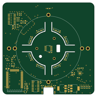
View base
81.2 × 81.2 mm81 parts2LApache-2.022.2k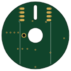
View screen
35 × 35 mm12 parts2LApache-2.022.2k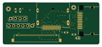
Display eval
byrantech
52.1 × 22.6 mm12 parts4LMIT4.3k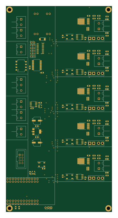
ChainlinkBase
98.4 × 190.5 mm119 parts2LApache-2.04.2k