
Eda pcb designer

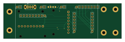
About the Eda pcb designer
Eda pcb designer is an open source PCB design by yupipi93, published on GitHub under the MIT license. It is a 2-layer board measuring 100 × 30 mm, with 13 components from 11 distinct parts.
Other key parts include the XIAO_left_socket, LSM6DSO32_SOCKET, BMP585_SOCKET, microSD_socket and XIAO_right_socket. By type, the board carries 5 ICs, 4 connectors, 2 resistors, 1 switch and 1 capacitor.
It belongs with the iot & wireless, power & battery and sensors designs in this gallery.
From the project
MultitecUA's open-source rocket avionics PCB for the SURT × SpainRocketry L1 launch (2026-07-18/19). 100 × 30 mm KiCad-9 board with a XIAO ESP32-S3 Plus, LSM6DSO32 IMU (±32 g), BMP585 barometer, microSD breakout, y un subsistema de batería v0.1.0 con switch de armado, jumper exte
MultitecUA's open-source rocket avionics PCB for the SURT × SpainRocketry L1 launch (2026-07-18/19). 100 × 30 mm KiCad-9 board with a XIAO ESP32-S3 Plus, LSM6DSO32 IMU (±32 g), BMP585 barometer, microSD breakout, y un subsistema de batería v0.1.0 con switch de armado, jumper externo y sensor de voltaje on-board. Diseñado end-to-end con el toolkit reusable pcb-designer — MT1 es su ejemplo dogfood.
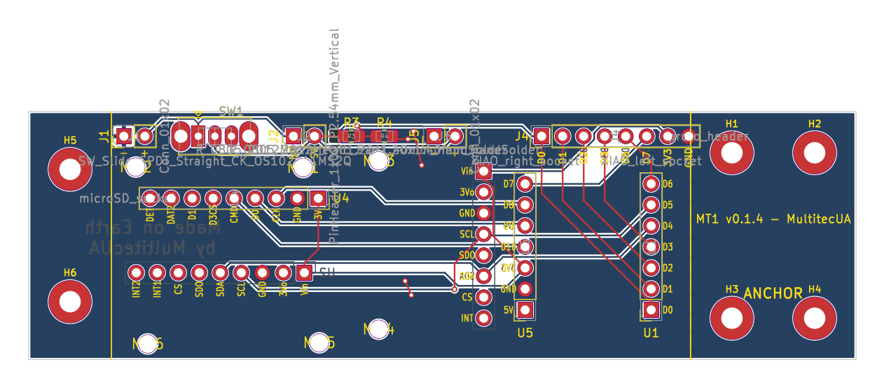
Main components on the Eda pcb designer
Eda pcb designer bill of materials (BOM)
13 components, 11 distinct parts — part numbers from the project's BOM.
| Qty | Part | Footprint | Refs |
|---|---|---|---|
| 1 | XIAO_left_socket | PinSocket_1x07_P2.54mm_Vertical | U1 |
| 1 | LSM6DSO32_SOCKET LSM6DSO32_socket | PinSocket_1x09_P2.54mm_Vertical | U2 |
| 1 | BMP585_SOCKET BMP585_socket | PinSocket_1x08_P2.54mm_Vertical | U3 |
| 1 | microSD_socket | PinSocket_1x09_P2.54mm_Vertical | U4 |
| 1 | XIAO_right_socket | PinSocket_1x07_P2.54mm_Vertical | U5 |
| 2 | Conn_01x02 | PinHeader_1x02_P2.54mm_Vertical | J1, J5 |
| 1 | PinHeader_1x02_P2.54mm_Vertical | PinHeader_1x02_P2.54mm_Vertical | J2 |
| 1 | proto_header | PinHeader_1x08_P2.54mm_Vertical | J4 |
| 1 | SW_Slide_SPDT_Straight_CK_OS102011MS2Q | SW_Slide_SPDT_Straight_CK_OS102011MS2Q | SW1 |
| 1 | 100NF C_0805_2012Metric_Pad1.18x1.45mm_HandSolder | C_0805_2012Metric_Pad1.18x1.45mm_HandSolder | C8 |
| 2 | 100K R_0805_2012Metric_Pad1.20x1.40mm_HandSolder | R_0805_2012Metric_Pad1.20x1.40mm_HandSolder | R3, R4 |
Eda pcb designer design files
The KiCad project lives in the yupipi93/eda-pcb-designer repository on GitHub; these links point at the commit this page was built from.
Eda pcb designer: common questions
How big is the Eda pcb designer?
The Eda pcb designer measures 100 × 30 mm, has 2 copper layers and is 1.6 mm thick.
How many components are on the Eda pcb designer?
13 components, from 11 distinct parts, with part numbers taken from the project's own BOM. The full bill of materials is listed on this page.
Where can I download the Eda pcb designer design files?
From the yupipi93/eda-pcb-designer repository on GitHub, which has the KiCad layout, the schematic and the BOM; the links under Design files point to each one.
Can I use the Eda pcb designer design in my own project?
Yes, under the terms of its MIT license, which yupipi93 chose for the repository.
Similar boards
Sensor smd
scottbez1
40 × 20 mm5 parts2LApache-2.04.2k
Sensors
StuckAtPrototype
15.2 × 9 mm14 parts4LApache-2.03.8k
Stack chan
stack-chan
50 × 50 mm33 parts2LApache-2.01.7k
Display Carrier
AxxAxx
35.6 × 58.2 mm5 parts2LGPL-3.01.7k
Microphone
Mentra-Community
5.5 × 6.1 mm6 parts2LMIT1.2k
Module 16S PassiveBalanceAddOn
stuartpittaway
61 × 74 mm86 parts2LCC-BY-NC-4.01.1k