
Sub 2 GHz Amplifier

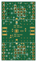
About the Sub 2 GHz Amplifier PCB
Sub 2 GHz Amplifier is an open source PCB design by akbar-q, published on GitHub. It is a 4-layer board measuring 28.6 × 49.5 mm, with 31 components from 17 distinct parts.
Other key parts include the LM317_SOT-223. By type, the board carries 9 capacitors, 4 resistors, 2 diodes, 2 inductors, 1 IC and 1 switch.
It belongs with the audio designs in this gallery.
From the project
The power supply design presented unique challenges, requiring a dual-rail configuration for simplified biasing while maintaining a compact 3mm height profile. The implementation delivers 500mA current capability with adjustable regulation and comprehensive filtering stages. A 4-
The power supply design presented unique challenges, requiring a dual-rail configuration for simplified biasing while maintaining a compact 3mm height profile. The implementation delivers 500mA current capability with adjustable regulation and comprehensive filtering stages. A 4-layer PCB design was chosen to optimize thermal management and signal integrity.
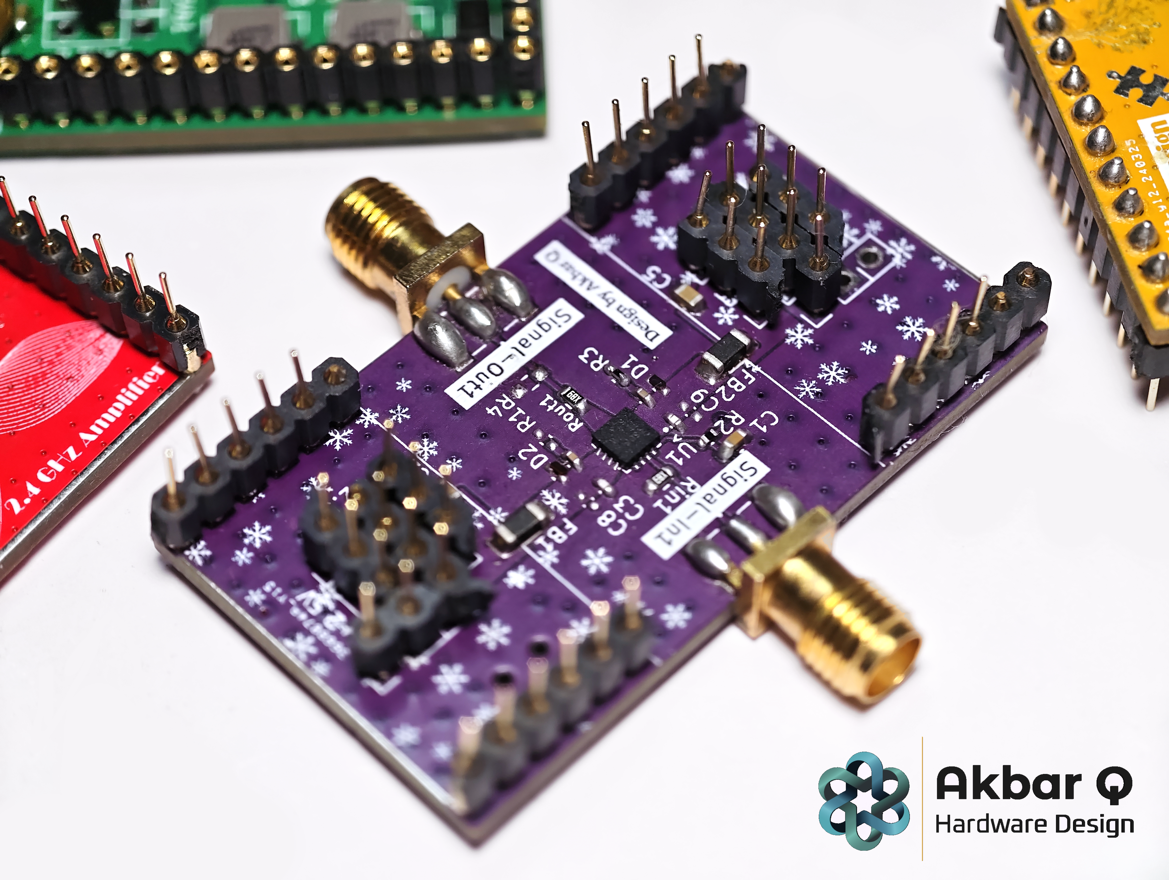
Main components on the Sub 2 GHz Amplifier
Sub 2 GHz Amplifier bill of materials (BOM)
31 components, 17 distinct parts — part numbers from the project's BOM.
| Qty | Part | Footprint | Refs |
|---|---|---|---|
| 1 | LM317_SOT-223 THS4302RGTT | QFN50P300X300X100-17N | U1 |
| 2 | Conn_01x02_Pin | PinHeader_1x02_P2.54mm_Vertical | +2.5V, -2.5V |
| 6 | Conn_01x03 | PinHeader_1x03_P2.54mm_Vertical | +G1, +G2, +G3, -G1, -G3, -G4 |
| 2 | 49.9 | R_0603_1608Metric | Rin1, Rout1 |
| 1 | SW_SPDT | SPDT-Long-SMD | SW1 |
| 2 | Conn_Coaxial | SMA_Samtec_SMA-J-P-X-ST-EM1_EdgeMount | Signal-In1, Signal-Out1 |
| 2 | ESD9B5.0ST5G | R_0402_1005Metric_Pad0.72x0.64mm_HandSolder | D1, D2 |
| 2 | FerriteBead_Small | R_1206_3216Metric_Pad1.30x1.75mm_HandSolder | FB1, FB2 |
| 1 | 2.2U 1u | C_0603_1608Metric_Pad1.08x0.95mm_HandSolder | C1 |
| 1 | 2.2U 22u | C_0603_1608Metric_Pad1.08x0.95mm_HandSolder | C2 |
| 2 | 2.2U 47p | C_0402_1005Metric_Pad0.74x0.62mm_HandSolder | C3, C6 |
| 2 | 2.2U 0.1u | C_0402_1005Metric_Pad0.74x0.62mm_HandSolder | C4, C7 |
| 1 | 100N 22u | C_0603_1608Metric_Pad1.08x0.95mm_HandSolder | C5 |
| 2 | 2.2U NP | C_0402_1005Metric_Pad0.74x0.62mm_HandSolder | C8, C9 |
| 2 | 680R 30.1 | R_0402_1005Metric_Pad0.72x0.64mm_HandSolder | R1, R3 |
| 1 | 680R JP | R_0402_1005Metric | R2 |
| 1 | 680R NP | R_0603_1608Metric_Pad0.98x0.95mm_HandSolder | R4 |
Sub 2 GHz Amplifier design files
The KiCad project lives in the akbar-q/Circuits-PCB-HardwareDesign repository on GitHub; these links point at the commit this page was built from.
Sub 2 GHz Amplifier: common questions
How big is the Sub 2 GHz Amplifier PCB?
The Sub 2 GHz Amplifier measures 28.6 × 49.5 mm, has 4 copper layers and is 1.6062 mm thick.
How many components are on the Sub 2 GHz Amplifier?
31 components, from 17 distinct parts, with part numbers taken from the project's own BOM. The full bill of materials is listed on this page.
Where can I download the Sub 2 GHz Amplifier design files?
From the akbar-q/Circuits-PCB-HardwareDesign repository on GitHub, which has the KiCad layout, the schematic and the BOM; the links under Design files point to each one.
Can I use the Sub 2 GHz Amplifier design in my own project?
The repository has no license, so all rights stay with akbar-q. Use it as a reference, and ask the author before reusing the design.
More boards in Circuits-PCB-HardwareDesign
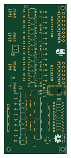
PLC RestoMod Digital I/O
68.7 × 164.9 mm132 parts2LNo license0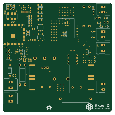 ESP32
MPPT-Controller
99 × 99 mm96 parts4LNo license0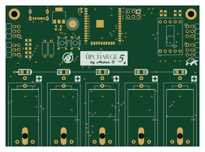 ESP32
020 NiMH Battery Charger
100 × 72.8 mm82 parts2LNo license0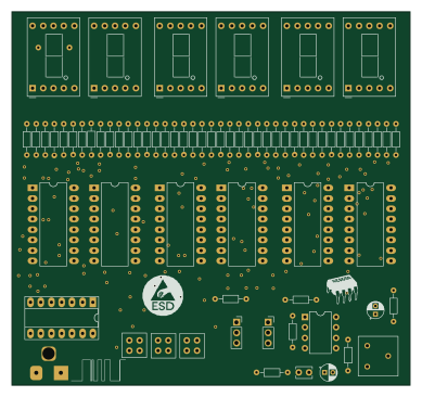
Practise PCB For Clock/Counter
97 × 91 mm67 parts2LNo license0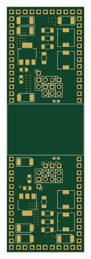
Linear Power Supply for Amplifier
28.6 × 91.2 mm60 parts4LNo license0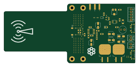
High Voltage Arc Detector
118.2 × 53.2 mm53 parts4LNo license0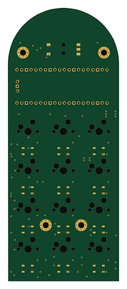 RP2040/RP2350
Macro Keypad w/ Rotary on Top
59.2 × 146.2 mm50 parts2LNo license0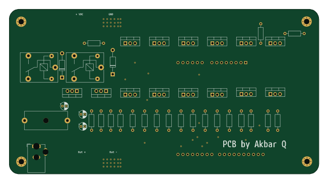 AVR/Arduino
Draft PCB for Potential Partnership for E-Bike Conversion
162.6 × 86.4 mm44 parts2LNo license0
Filter Plate to Cover Power
28.6 × 20.4 mm3 parts2LNo license0
Similar boards
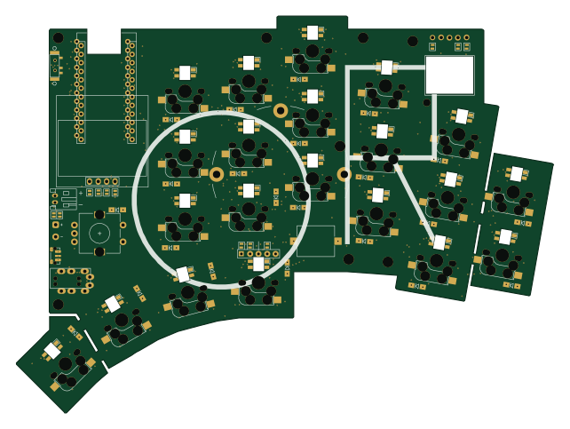
KLOR
GEIGEIGEIST
160.2 × 118.3 mm79 parts2LGPL-3.01.2k
USB
shanteacontrols
52 × 12.6 mm6 parts2LApache-2.0956
Pots
390 × 93 mm75 parts2LApache-2.0956
ButtonsLEDs
390 × 37 mm82 parts2LApache-2.0956
PicoGUS Hand386
polpo
29.2 × 75.2 mm43 parts4LGPL-2.0800
Snark barker
schlae
231.1 × 106.7 mm193 parts2LNo license687