
Inki l2

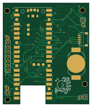
About the Inki l2 PCB
Inki l2 is an open source Raspberry Pi PCB design by c0de111, published on GitHub under the Apache-2.0 license. It is a 2-layer board measuring 47.2 × 55.5 mm, with 60 components from 40 distinct parts.
Its main chip is the SC0918, from the Raspberry Pi family. Other key parts include the BMP581, RV-3028 and ST25. By type, the board carries 22 resistors, 13 capacitors, 11 diodes, 5 connectors, 4 transistors and 3 ICs.
It belongs with the iot & wireless, displays & leds and power & battery designs in this gallery.
From the project
Battery-powered e-paper sign: room signage, sensor graphs, home automation, or anything over Wi-Fi. Wakes by real-time clock, NFC tap, or button. Raspberry Pi Pico W firmware, custom PCB, and 3D-printed case included.
This directory contains the schematic and hardware documentation for the Tinta PCB. There is also a former hand-solderable design, see legacy/.
The Tinta circuit is designed for long-term operation (years) using 3×AAA or 3×AA batteries. It uses a real-time clock for accurate timekeeping and wake-up scheduling — either a DS3231 or RV-3028, detected automatically at runtime — combined with MOSFET-based power switching to fully disconnect the controller between wake cycles. During wake cycles, information is fetched via Wi-Fi and displayed on an ePaper display that retains its content without…
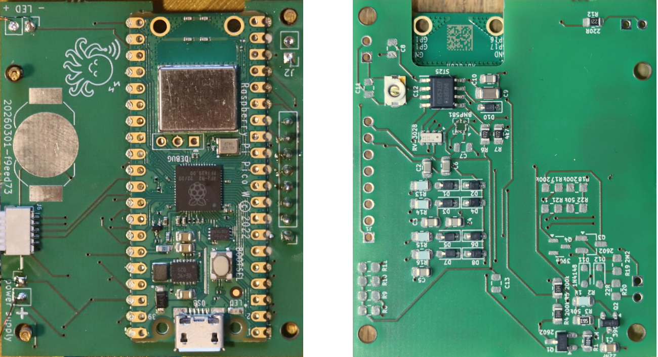
Main components on the Inki l2
Inki l2 bill of materials (BOM)
60 components, 40 distinct parts — part numbers from the project's BOM.
| Qty | Part | Footprint | Refs |
|---|---|---|---|
| 1 | BMP581 | BMP581 | U2 |
| 1 | RV-3028 | MicroCrystal_C7_SON-8_1.5x3.2mm_P0.9mm | U4 |
| 1 | ST25 | SOIC127P600X175-8N | U5 |
| 2 | TSM260P02CX 2602 | SOT-23_Handsoldering | Q1, Q3 |
| 2 | MMBT3904 3904 | SOT-23 | Q2, Q4 |
| 1 | connector epaper | PinHeader_1x08_P2.54mm_Vertical | J1 |
| 1 | CONN_01X02_SOCKET antenna | PinHeader_1x02_P2.54mm_Vertical | J2 |
| 1 | CONN_01X02_SOCKET Battery 3xAA/AAA | PinHeader_1x02_P2.54mm_Vertical | J3 |
| 1 | pushbuttons | JST_SH_SM05B-SRSS-TB_1x05-1MP_P1.00mm_Horizontal | J6 |
| 1 | CONN_01X02_SOCKET status LED | PinHeader_1x02_P2.54mm_Vertical | J7 |
| 1 | Coin Cell (RTC Backup) | BatteryHolder_LINX_BAT-HLD-012-SMT | BT1 |
| 1 | SC0918 | RaspberryPi_Pico_W_SMD | pico1 |
| 7 | BAT54J | D_SOD-323_HandSoldering | D1, D3, D4, D5, D6, D7, D8 |
| 1 | 1N4148WS BAT54J | D_SOD-323_HandSoldering | D2 |
| 2 | BAT54J | D_SOD-323_HandSoldering | D10, D11 |
| 1 | 1N4148 | D_SOD-323_HandSoldering | D12 |
| 1 | 100NF 22nF | C_0805_2012Metric | C1 |
| 7 | 100NF 100nF | C_0805_2012Metric | C2, C3, C4, C5, C6, C7, C8 |
| 1 | 4.7uF | C_1206_3216Metric | C9 |
| 2 | 100nF | C_0805_2012Metric | C10, C13 |
Show 20 more
| Qty | Part | Footprint | Refs |
|---|---|---|---|
| 1 | 10pF | C_0805_2012Metric | C11 |
| 1 | JZ400 | JZ400 | C12 |
| 1 | 200K 1M | R_0805_2012Metric_Pad1.20x1.40mm_HandSolder | R1 |
| 3 | 1k | R_0805_2012Metric_Pad1.20x1.40mm_HandSolder | R2, R13, R21 |
| 1 | 4K7 50k | R_0805_2012Metric_Pad1.20x1.40mm_HandSolder | R3 |
| 1 | 4K7 200k | R_0805_2012Metric_Pad1.20x1.40mm_HandSolder | R4 |
| 1 | 200k | R_0805_2012Metric_Pad1.20x1.40mm_HandSolder | R5 |
| 1 | 220R 4k7 | R_0805_2012Metric_Pad1.20x1.40mm_HandSolder | R6 |
| 1 | 200K 4k7 | R_0805_2012Metric_Pad1.20x1.40mm_HandSolder | R7 |
| 1 | 200K 10k | R_0805_2012Metric_Pad1.20x1.40mm_HandSolder | R8 |
| 1 | 50K 10k | R_0805_2012Metric_Pad1.20x1.40mm_HandSolder | R9 |
| 2 | 10k | R_0805_2012Metric_Pad1.20x1.40mm_HandSolder | R10, R11 |
| 1 | 220R | R_0805_2012Metric_Pad1.20x1.40mm_HandSolder | R12 |
| 1 | 200K 1k | R_0805_2012Metric_Pad1.20x1.40mm_HandSolder | R14 |
| 1 | 2M2 1k | R_0805_2012Metric_Pad1.20x1.40mm_HandSolder | R15 |
| 1 | 22R 1k | R_0805_2012Metric_Pad1.20x1.40mm_HandSolder | R16 |
| 2 | 10K 200k | R_0805_2012Metric_Pad1.20x1.40mm_HandSolder | R17, R18 |
| 1 | 10K 2M2 | R_0805_2012Metric_Pad1.20x1.40mm_HandSolder | R19 |
| 1 | 10K 22R | R_0805_2012Metric_Pad1.20x1.40mm_HandSolder | R20 |
| 1 | 50K 50k | R_0805_2012Metric_Pad1.20x1.40mm_HandSolder | R22 |
Inki l2 design files
The KiCad project lives in the c0de111/tinta repository on GitHub; these links point at the commit this page was built from.
Inki l2: common questions
What microcontroller does the Inki l2 use?
The Inki l2 is built around the SC0918, from the Raspberry Pi family.
How big is the Inki l2 PCB?
The Inki l2 measures 47.2 × 55.5 mm, has 2 copper layers and is 1.6 mm thick.
How many components are on the Inki l2?
60 components, from 40 distinct parts, with part numbers taken from the project's own BOM. The full bill of materials is listed on this page.
Where can I download the Inki l2 design files?
From the c0de111/tinta repository on GitHub, which has the KiCad layout, the schematic and the BOM; the links under Design files point to each one.
Can I use the Inki l2 design in my own project?
Yes, under the terms of its Apache-2.0 license, which c0de111 chose for the repository.
Can I test firmware for the Inki l2 without the hardware?
Yes. HardLabs builds a simulation of the board from its netlist and BOM, so you can run and debug Raspberry Pi firmware against it before you order a PCB.
More boards in tinta
Similar boards
 Raspberry Pi
Haxo hw
cardonabits
102.4 × 211.3 mm38 parts2LCustom license672 Raspberry Pi
Desktop 50 Pin TopConn
BlueSCSI
89.2 × 82.6 mm103 parts2LGPL-3.0449 Raspberry Pi
PowerBook
74.5 × 56.3 mm78 parts2LGPL-3.0449 Raspberry Pi
BitDogLab 5.4
BitDogLab
87.9 × 123.9 mm56 parts2LCERN-OHL-S-2.0201 Raspberry Pi
BitDogLab Main SMD version
87.9 × 98.7 mm124 parts2LCERN-OHL-S-2.0201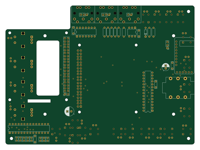 Raspberry Pi
Zynthian mini v2 20 buttons short
zynthian
163 × 120 mm87 parts2LNo license154