
Hdmi edp2

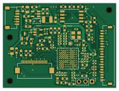
About the Hdmi edp2 PCB
Hdmi edp2 is an open source PCB design by cetola, published on GitHub. It is a 4-layer board measuring 43.5 × 32.5 mm, with 93 components from 33 distinct parts.
Other key parts include the LP2985A-25DBVT, LM2830XQMFE/NOPB, STDP2600AD and W25Q32JVSS. By type, the board carries 45 capacitors, 31 resistors, 6 inductors, 4 ICs, 4 connectors and 1 transistor.
It belongs with the audio and power & battery designs in this gallery.
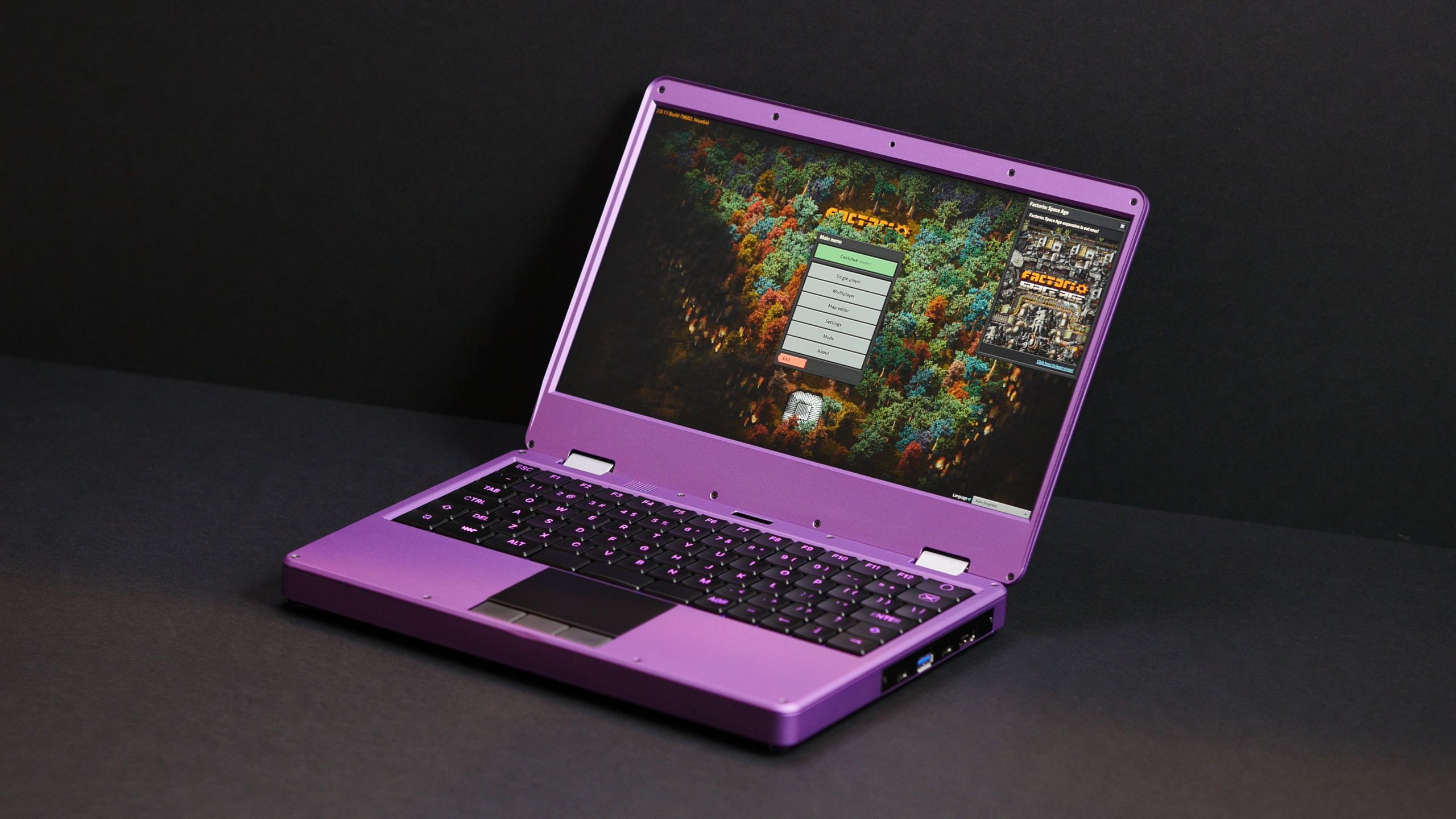
From the project
The original Open Hardware laptop, reloaded.
The original Open Hardware laptop, reloaded.
MNT Reform Next takes the MNT Reform family's modular approach a few steps further: The motherboard doesn't have any exterior ports, instead it breaks out all important signals in groups to FPC and JST-SH headers. The connectivity to the outside is implemented via user-exchangable Port Boards that increase repairability, customizability and future proofing of interfaces. The motherboard provides the system controller (RP2040 based), main (multi chemistry) LiFePO4/LiIon charger buck/boost controller, main 5V and 3V3 power rails and the SOM…
Main components on the Hdmi edp2
Hdmi edp2 bill of materials (BOM)
93 components, 33 distinct parts.
| Qty | Part | Footprint | Refs |
|---|---|---|---|
| 1 | LP2985A-25DBVT Texas Instruments | SOT-23-5 | U1 |
| 1 | LM2830XQMFE/NOPB Texas Instruments | SOT-23-5 | U2 |
| 1 | STDP2600AD Kinetic | BGA81C80P9X9_800X800X140N | U3 |
| 1 | W25Q32JVSS Winbond | SOIC-8W_5.3x5.3mm_P1.27mm | U4 |
| 1 | 2N7002-T1-E3 Vishay / Siliconix | SOT-23 | Q1 |
| 1 | ABM8-27.000MHZ-B2-T Abracon | Crystal_SMD_3225-4Pin_3.2x2.5mm | Y1 |
| 1 | Conn_01x20 Hirose | Hirose_FH12-20S-0.5SH_1x20-1MP_P0.50mm_Horizontal | J1 |
| 1 | Conn_UART DNP | PinHeader_1x03_P2.54mm_Vertical | J2 |
| 1 | DISP JST | JST_SH_SM06B-SRSS-TB_1x06-1MP_P1.00mm_Horizontal | J4 |
| 1 | Conn_01x20 JST | JST_SHL_SM20B-SHLS-TF_1x20-1MP_P1.00mm_Horizontal | J5 |
| 1 | PMEG1020EA,115 Nexperia | D_SOD-323 | D1 |
| 5 | FerriteBead_Small Laird | R_0603_1608Metric | FB1, FB2, FB3, FB4, FB5 |
| 1 | 3.3uH Murata | L_1210_3225Metric | L1 |
| 2 | 10uF Samsung | C_0603_1608Metric | C1, C8 |
| 2 | 4.7uF Kyocera AVX | C_0402_1005Metric | C2, C4 |
| 1 | 10nF Kyocera AVX | C_0402_1005Metric | C3 |
| 3 | 22pF Yageo | C_0402_1005Metric | C5, C6, C18 |
| 18 | 0.1uF Kyocera AVX | C_0402_1005Metric | C7, C24, C25, C26, C27, C28, C29, C30 +10 |
| 8 | 10uF Kyocera AVX | C_0402_1005Metric | C9, C10, C11, C12, C13, C14, C15, C16 |
| 1 | 1uF Yageo | C_0402_1005Metric | C17 |
Show 13 more
| Qty | Part | Footprint | Refs |
|---|---|---|---|
| 5 | 0.47uF KEMET | C_0402_1005Metric | C19, C20, C21, C22, C23 |
| 3 | 10pF Yageo | C_0402_1005Metric | C33, C34, C35 |
| 2 | 47uF Kyocera AVX | C_0805_2012Metric | C41, C44 |
| 1 | 20k Vishay Dale | R_0603_1608Metric | R1 |
| 6 | 0 Yageo | R_0603_1608Metric | R2, R7, R8, R23, R25, R29 |
| 6 | 100k Yageo | R_0603_1608Metric | R3, R5, R10, R11, R12, R39 |
| 5 | 15k 1% Vishay Dale | R_0603_1608Metric | R13, R14, R27, R28, R30 |
| 1 | 10k 1% Yageo | R_0603_1608Metric | R15 |
| 2 | 249 1% Bourns | R_0603_1608Metric | R16, R20 |
| 3 | 3k Yageo | R_0603_1608Metric | R17, R31, R32 |
| 2 | DNP DNP | R_0603_1608Metric | R18, R38 |
| 4 | 4.7k Vishay Dale | R_0603_1608Metric | R21, R22, R36, R37 |
| 1 | 47k Vishay Dale | R_0603_1608Metric | R35 |
Hdmi edp2 design files
The KiCad project lives in the cetola/reform-next-mirror repository on GitHub; these links point at the commit this page was built from.
- Layouthdmi-edp2/hdmi-edp2.kicad_pcb
- Schematichdmi-edp2/hdmi-edp2.kicad_sch
Hdmi edp2: common questions
How big is the Hdmi edp2 PCB?
The Hdmi edp2 measures 43.5 × 32.5 mm, has 4 copper layers and is 1 mm thick.
How many components are on the Hdmi edp2?
93 components, from 33 distinct parts. The full bill of materials is listed on this page.
Where can I download the Hdmi edp2 design files?
From the cetola/reform-next-mirror repository on GitHub, which has the KiCad layout and the schematic; the links under Design files point to each one.
Can I use the Hdmi edp2 design in my own project?
The repository has no license, so all rights stay with cetola. Use it as a reference, and ask the author before reusing the design.
More boards in reform-next-mirror
 RP2040/RP2350
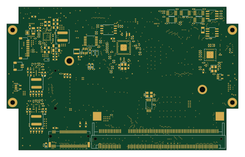
Nref motherboard
122.6 × 75.9 mm269 parts6LNo license0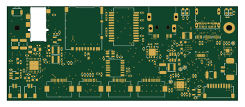
Nref ports one
88 × 35.9 mm146 parts4LNo license0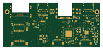
Nref ports two
87.5 × 40.2 mm137 parts4LNo license0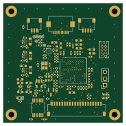
Reform camera
46 × 46 mm114 parts4LNo license0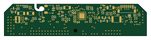
Nref batterypack
75 × 17 mm83 parts4LNo license0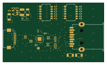
Nref usb3-redriver
54.5 × 32 mm40 parts4LNo license0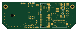
Nref wifi m2
66 × 24 mm28 parts4LNo license0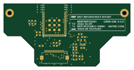
Nref wifi
66 × 33 mm23 parts2LNo license0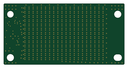
Trackpad IQS9150
105.5 × 53.3 mm10 parts2LNo license0
Nref batterypack backside
75 × 17 mm3 parts4LNo license0
Similar boards

Stack chan
stack-chan
50 × 50 mm33 parts2LApache-2.01.7k
Display Carrier
AxxAxx
35.6 × 58.2 mm5 parts2LGPL-3.01.7k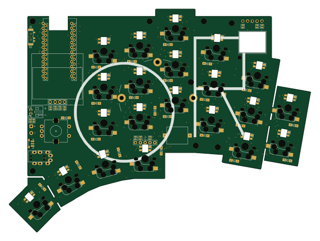
KLOR
GEIGEIGEIST
160.2 × 118.3 mm79 parts2LGPL-3.01.2k
ControllerCurrentShuntAddOn
stuartpittaway
26 × 16.9 mm9 parts2LCC-BY-NC-4.01.1k
Module 16S PassiveBalanceAddOn
61 × 74 mm86 parts2LCC-BY-NC-4.01.1k
TemperaturePCB PANEL
116 × 75.5 mm178 parts2LCC-BY-NC-4.01.1k