
HackBadge

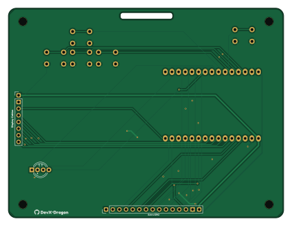
About the HackBadge PCB
HackBadge is an open source ESP32 PCB design by DevX-Dragon, published on GitHub. It is a 2-layer board measuring 105 × 80 mm, with 7 components from 7 distinct parts.
Its main chip is the ESP32_DevKit_V1_DOIT_30GPIOs, from the ESP32 family. By type, the board carries 4 switches, 2 connectors and 1 module.
It belongs with the iot & wireless and displays & leds designs in this gallery.
From the project
- ESP32 Microcontroller: Integrated with WI-FI and Bluetooth LE (BLE) for networking, mesh communication, and OTA updates. - 4.2 inch Waveshare E-Paper Display: Ultra low-power, high visibility display that retains text and images even its powered off. - Programmale buttons: Dedi
- ESP32 Microcontroller: Integrated with WI-FI and Bluetooth LE (BLE) for networking, mesh communication, and OTA updates. - 4.2 inch Waveshare E-Paper Display: Ultra low-power, high visibility display that retains text and images even its powered off. - Programmale buttons: Dedicated input buttons for navigating menus, switching displays or triggering a custom action. - Expaned GPIO Breakout: Exposed GPIO pins allowing easy access for external sesors, LEDs and modules.
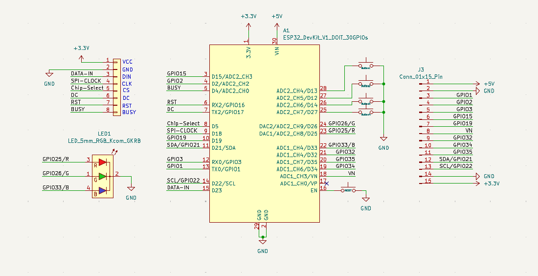
Main components on the HackBadge
HackBadge bill of materials (BOM)
7 components, 7 distinct parts.
| Qty | Part | Footprint | Refs |
|---|---|---|---|
| 1 | ESP32_DevKit_V1_DOIT_30GPIOs | DOIT_ESP32_DEVKIT_30Pins | A1 |
| 1 | Conn_01x08 | PinHeader_1x08_P2.54mm_Vertical | J1 |
| 1 | Conn_01x15_Pin | PinHeader_1x15_P2.54mm_Vertical | J3 |
| 1 | Button1 | SW_PUSH_6mm_H5mm | SW5 |
| 1 | Button2 | SW_PUSH_6mm_H5mm | SW6 |
| 1 | Button3 | SW_PUSH_6mm_H5mm | SW7 |
| 1 | Button4 | SW_PUSH_6mm_H5mm | SW8 |
HackBadge design files
The KiCad project lives in the DevX-Dragon/HackBadge repository on GitHub; these links point at the commit this page was built from.
HackBadge: common questions
What microcontroller does the HackBadge use?
The HackBadge is built around the ESP32_DevKit_V1_DOIT_30GPIOs, from the ESP32 family.
How big is the HackBadge PCB?
The HackBadge measures 105 × 80 mm, has 2 copper layers and is 1.6 mm thick.
How many components are on the HackBadge?
7 components, from 7 distinct parts. The full bill of materials is listed on this page.
Where can I download the HackBadge design files?
From the DevX-Dragon/HackBadge repository on GitHub, which has the KiCad layout and the schematic; the links under Design files point to each one.
Can I use the HackBadge design in my own project?
The repository has no license, so all rights stay with DevX-Dragon. Use it as a reference, and ask the author before reusing the design.
Can I test firmware for the HackBadge without the hardware?
Yes. HardLabs builds a simulation of the board from its netlist and BOM, so you can run and debug ESP32 firmware against it before you order a PCB.
Similar boards
 ESP32
OSO-BOOK-B1
joeycastillo
85 × 115 mm65 parts2LCC-BY-SA-4.08.1k ESP32
Powertrain
byrantech
64 × 45.4 mm171 parts4LMIT4.3k ESP32
Badge
atopile
56.3 × 39 mm239 parts4LMIT4.0k ESP32
Esp32 minimal
36.2 × 26.8 mm20 parts2LMIT4.0k ESP32
Racer
StuckAtPrototype
36 × 50.2 mm70 parts4LApache-2.03.8k ESP32
Controller
29 × 74 mm58 parts4LApache-2.03.8k