
NES backup

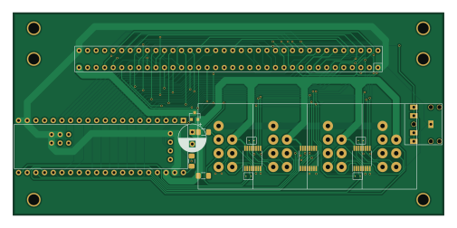
About the NES backup PCB
NES backup is an open source PCB design by digilogistist, published on GitHub under the CC0-1.0 license. It is a 2-layer board measuring 126 × 59.2 mm, with 15 components from 14 distinct parts.
Other key parts include the 74AHCT1G125, BLUE_PILL, 4052 and 4053. By type, the board carries 6 connectors, 4 ICs, 3 resistors, 1 transistor and 1 capacitor.
It belongs with the retro computing designs in this gallery.
From the project
USB-NES and NES-FASTGFX product engineering repository
Brad Taylor BTTD Group 04/05/2023 https://usbnes.com
- Source code - Firmware binaries (composite and discrete) - PCB engineering files (USB-NES, NES-BACKUP and new NES-FASTGFX) - Serial wire debug wiring diagram - Technical documentations - Quick setup guide print-out - DIY kit guide print-out (manufacturing instructions) - Owner's manual PDF - 3D case models - Manufacturing BOMs and part source links - Photo gallery
Main components on the NES backup
NES backup bill of materials (BOM)
15 components, 14 distinct parts — part numbers from the project's BOM.
| Qty | Part | Footprint | Refs |
|---|---|---|---|
| 1 | 74AHCT1G125 4052 | TSSOP-16_4.4x5mm_P0.65mm | U1 |
| 1 | BLUE_PILL | blue_pill | U2 |
| 1 | 4052 | TSSOP-16_4.4x5mm_P0.65mm | U3 |
| 1 | 4053 | TSSOP-16_4.4x5mm_P0.65mm | U4 |
| 1 | TSM500P02CX | SOT-23 | Q1 |
| 1 | NES-CART | NES_CART | J1 |
| 1 | MINI_PHONE_PLUG | MINI_PHONE_PLUG | J2 |
| 1 | PAD 0 | NES_pad_plug | J3 |
| 1 | PAD 1 | NES_pad_plug | J4 |
| 1 | PAD 2 | NES_pad_plug | J5 |
| 1 | PAD 3 | NES_pad_plug | J6 |
| 1 | CP | CP_Radial_D8.0mm_P3.50mm | C1 |
| 1 | RR0510P-103-D 10K | R_1206_3216Metric_Pad1.42x1.75mm_HandSolder | R1 |
| 2 | 10K | R_1206_3216Metric_Pad1.42x1.75mm_HandSolder | R2, R3 |
NES backup design files
The KiCad project lives in the digilogistist/The-Open-Source-USB-NES-Project repository on GitHub; these links point at the commit this page was built from.
NES backup: common questions
How big is the NES backup PCB?
The NES backup measures 126 × 59.2 mm, has 2 copper layers and is 1.6 mm thick.
How many components are on the NES backup?
15 components, from 14 distinct parts, with part numbers taken from the project's own BOM. The full bill of materials is listed on this page.
Where can I download the NES backup design files?
From the digilogistist/The-Open-Source-USB-NES-Project repository on GitHub, which has the KiCad layout and the BOM; the links under Design files point to each one.
Can I use the NES backup design in my own project?
Yes, under the terms of its CC0-1.0 license, which digilogistist chose for the repository.
More boards in The-Open-Source-USB-NES-Project
Similar boards
Amiga External
hoglet67
21.9 × 76.7 mm6 parts2LGPL-3.01.0k
Atari pickup
26.4 × 53.9 mm7 parts2LGPL-3.01.0k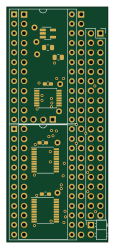
Deniseadapter
26.7 × 62.2 mm16 parts2LGPL-3.01.0k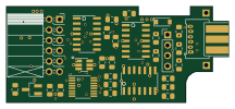
Analog
53.9 × 23.2 mm33 parts2LGPL-3.01.0k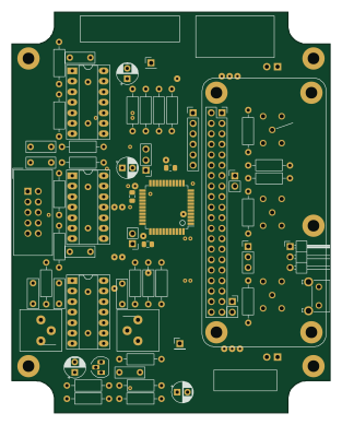
Rgb to hdmi
77 × 97 mm67 parts2LGPL-3.01.0k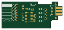
Buffer
53.9 × 23.2 mm13 parts2LGPL-3.01.0k