
Programming jig

About the Programming jig PCB
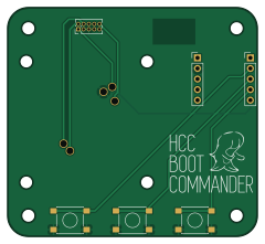
Programming jig is an open source PCB design by GJN-Aerospace, published on GitHub. It is a 2-layer board measuring 60 × 55 mm, with 11 components from 11 distinct parts.
Other key parts include the SW1, SW2 and SW3. By type, the board carries 8 connectors and 3 ICs.
It belongs with the robotics & motion designs in this gallery.
From the project
GitHub repository for actively stabilized model rocket project.
Main components on the Programming jig
Programming jig bill of materials (BOM)
11 components, 11 distinct parts.
| Qty | Part | Footprint | Refs |
|---|---|---|---|
| 1 | SW1 | SW_SPST_PTS645 | U1 |
| 1 | SW2 | SW_SPST_PTS645 | U2 |
| 1 | SW3 | SW_SPST_PTS645 | U3 |
| 1 | Trinket_Left | Pin_Header_Straight_1x05_Pitch2.54mm | J1 |
| 1 | Trinket_Right | Pin_Header_Straight_1x05_Pitch2.54mm | J2 |
| 1 | 3V3 | POGO_PIN | J3 |
| 1 | GND | POGO_PIN | J4 |
| 1 | RST | POGO_PIN | J5 |
| 1 | SWDIO | POGO_PIN | J6 |
| 1 | SWCLK | POGO_PIN | J7 |
| 1 | DBG_CONN | Pin_Header_Straight_2x05_Pitch1.27mm | P1 |
Programming jig design files
The KiCad project lives in the GJN-Aerospace/Halcyon repository on GitHub; these links point at the commit this page was built from.
Programming jig: common questions
How big is the Programming jig PCB?
The Programming jig measures 60 × 55 mm, has 2 copper layers and is 1.6 mm thick.
How many components are on the Programming jig?
11 components, from 11 distinct parts. The full bill of materials is listed on this page.
Where can I download the Programming jig design files?
From the GJN-Aerospace/Halcyon repository on GitHub, which has the KiCad layout; the links under Design files point to each one.
Can I use the Programming jig design in my own project?
The repository has no license, so all rights stay with GJN-Aerospace. Use it as a reference, and ask the author before reusing the design.
More boards in Halcyon
 Microchip SAM
Halcyon
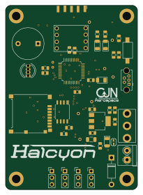
50 × 70 mm70 parts2LNo license0 Microchip SAM
Hccg
18 × 22 mm25 parts2LNo license0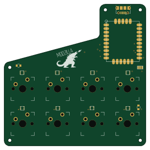 Microchip SAM
Hcc cherry
77 × 77 mm21 parts2LNo license0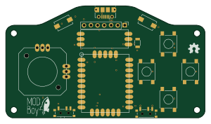 Microchip SAM
Hcc boy
75 × 42.3 mm15 parts2LNo license0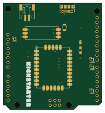 Microchip SAM
Hcc arduino
53.3 × 57.6 mm12 parts2LNo license0
Lipo charge mod
18 × 7 mm9 parts2LNo license0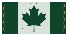 Microchip SAM
Cad flag
70 × 35 mm4 parts2LNo license0
Similar boards
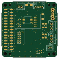
Stack chan
stack-chan
50 × 50 mm33 parts2LApache-2.01.7k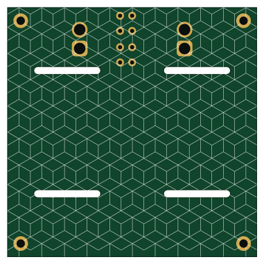
Cube batteryboard
willem-pennings
95 × 95 mm4 parts2LGPL-3.01.1k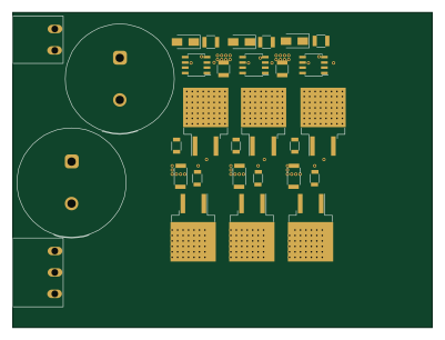
Trollerv2
rene-dev
100 × 75 mm33 parts4LGPL-3.0979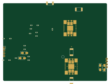
Powerstep
95.2 × 71.5 mm28 parts4LGPL-3.0979
11ua
57.3 × 19 mm26 parts2LGPL-3.0979
Diff driver
32 × 22 mm14 parts2LGPL-3.0979