
CORE

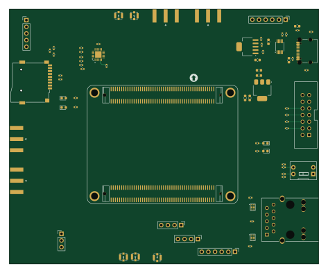
About the CORE PCB
CORE is an open source FPGA PCB design by Han-ZenX, published on GitHub under the Custom license license. It is a 4-layer board measuring 118 × 97 mm, with 81 components from 34 distinct parts.
Its main chip is the ZYNQ7010&7020, from the FPGA family. Other key parts include the TXS02612RTWR, TPS78633, SD_Card, IPEX1 and AMS1117-1.8. By type, the board carries 30 resistors, 18 capacitors, 12 connectors, 10 ICs, 6 diodes and 1 module.
From the project
The core computing module of high-end frequency meters
本项目是高端频率计的核心计算模块,基于 Xilinx ZYNQ7020 核心板实现高精度频率测量。系统采用 FPGA 采集 + DDR 存储 + ARM 计算 的异构协同架构,充分发挥 ZYNQ 平台 PL(可编程逻辑)与 PS(处理系统)协同工作的优势,实现高精度、高实时性的频率测量。
- FPGA 采集:利用 PL 端实现高速信号采集与精密计数,保证测量闸门时间的硬件级精度 - DDR 存储:采集数据经 AXI 总线高速写入 DDR,实现大容量、连续测量数据缓存 - ARM 计算:PS 端运行本仓库固件,完成数据处理、频率解算与结果输出
Main components on the CORE
CORE bill of materials (BOM)
81 components, 34 distinct parts.
| Qty | Part | Footprint | Refs |
|---|---|---|---|
| 1 | TXS02612RTWR | QFN24_RTW | U1 |
| 1 | TPS78633 | SOT-223-6 | U2 |
| 1 | SD_Card | SIM-SMD_LX_XDFP-0090-012 | U3 |
| 5 | IPEX1 | JLC_IPEX-1 | U4, U8, U9, U10, U11 |
| 1 | AMS1117-1.8 | SOT-223-3_TabPin2 | U5 |
| 1 | CH340E Microchip Tech | MSOP-10_3x3mm_P0.5mm | U6 |
| 1 | ZYNQ7010&7020 | ZYNQ7010&7020_CB | M1 |
| 2 | Conn_01x06_Socket | PinHeader_1x06_P2.54mm_Vertical | J1, J11 |
| 4 | Conn_Coaxial | SMA_Amphenol_132289_EdgeMount | J2, J3, J4, J5 |
| 1 | USB_C_Receptacle_USB2.0_16P | USB_C_Receptacle_Palconn_UTC16-G | J10 |
| 3 | Conn_01x04_Socket | PinHeader_1x04_P2.54mm_Vertical | J13, J16, J26 |
| 1 | Conn_01x03_Socket | PinHeader_1x03_P2.54mm_Vertical | J14 |
| 1 | Conn_01x05_Socket | PinHeader_1x05_P2.54mm_Vertical | J15 |
| 1 | CSW-2P | CSW DIP-2P | BOOT_CFG1 |
| 1 | HR911131A | HR911131A | GE_PS1 |
| 1 | JTAG | DC3_14P_2_7_DIP | JTAG1 |
| 1 | RGBLCD | FPC-TOP40 | RGB TFTLCD1 |
| 2 | AZ1143-04F.R7G | DFN2510P10E | D1, D2 |
| 4 | LED | LED_0603_1608Metric | D3, D4, D5, D6 |
| 7 | 100nF | C_0402_1005Metric | C1, C2, C3, C5, C6, C11, C19 |
Show 14 more
| Qty | Part | Footprint | Refs |
|---|---|---|---|
| 1 | 10uF | C_0402_1005Metric | C4 |
| 6 | 10uF | C_0603_1608Metric | C7, C8, C10, C12, C15, C17 |
| 1 | 10nF | C_0402_1005Metric | C9 |
| 1 | 1nF | C_0402_1005Metric | C13 |
| 2 | 100nF | C_0603_1608Metric | C16, C18 |
| 4 | 33R | R_0402_1005Metric | R1, R2, R3, R4 |
| 6 | 499R | R_0402_1005Metric | R5, R6, R7, R8, R9, R10 |
| 2 | 20K | R_0402_1005Metric | R11, R12 |
| 3 | 10K | R_0402_1005Metric | R13, R14, R18 |
| 6 | 4.7K | R_0402_1005Metric | R15, R19, R20, R21, R22, R23 |
| 1 | 330 | R_0402_1005Metric | R16 |
| 4 | 0 | R_0402_1005Metric | R17, R38, R39, R40 |
| 2 | 5.1K | R_0402_1005Metric | R36, R37 |
| 2 | 49.9 | R_0402_1005Metric | R41, R42 |
CORE design files
The KiCad project lives in the Han-ZenX/CORE repository on GitHub; these links point at the commit this page was built from.
CORE: common questions
What microcontroller does the CORE use?
The CORE is built around the ZYNQ7010&7020, from the FPGA family.
How big is the CORE PCB?
The CORE measures 118 × 97 mm, has 4 copper layers and is 1.6062 mm thick.
How many components are on the CORE?
81 components, from 34 distinct parts. The full bill of materials is listed on this page.
Where can I download the CORE design files?
From the Han-ZenX/CORE repository on GitHub, which has the KiCad layout and the schematic; the links under Design files point to each one.
Can I use the CORE design in my own project?
It is published under Custom license, which limits how it may be reused; read the license before building on it.
Can I test firmware for the CORE without the hardware?
Yes. HardLabs builds a simulation of the board from its netlist and BOM, so you can run and debug FPGA firmware against it before you order a PCB.
Similar boards
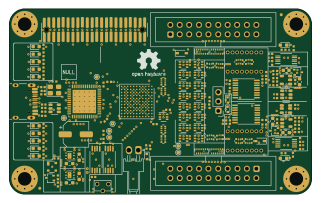 FPGA
FPGABase board
GlasgowEmbedded
80 × 49 mm222 parts4L0BSD2.2k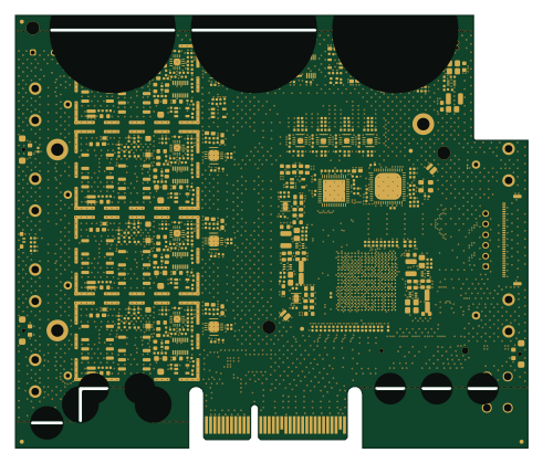 FPGA
FPGAThunderscope Rev5.3
EEVengers
122.5 × 103.5 mm817 parts6LMIT1.3k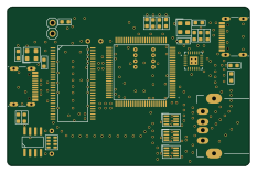 FPGA
FPGAUsb sniffer
ataradov
58.2 × 38.1 mm86 parts2LBSD-3-Clause1.3k FPGA
FPGATomu, I'm
theacodes
13 × 9.4 mm40 parts4LMIT1.1k FPGA
FPGAIcepi zero
cheyao
65 × 30 mm143 parts4LSHL-2.1828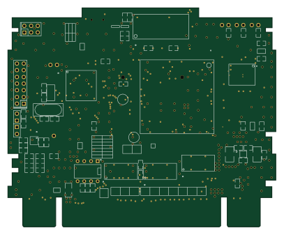 FPGA
FPGASd2snes
mrehkopf
101.5 × 83 mm147 partsGPL-2.0717