
Pn5180 carrier

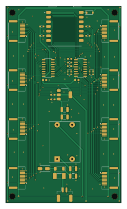
About the Pn5180 carrier PCB
Pn5180 carrier is an open source ESP32 PCB design by hyiger, published on GitHub. It is a 2-layer board measuring 62.5 × 106.5 mm, with 35 components from 26 distinct parts.
Its main chip is the XIAO ESP32C6, from the ESP32 family. Other key parts include the SN74HC138DR, SN74HC151DR, TLV1117LV33DCYR and MP1584EN mini buck module. By type, the board carries 9 connectors, 9 resistors, 8 capacitors, 5 ICs, 3 diodes and 1 fuse.
It belongs with the dev boards & breakouts designs in this gallery.
From the project
PN5180 8-bay NFC reader carrier board for a filament spool rack (KiCad 10, XIAO ESP32C6)
Carrier board that lets 4 or 8 PN5180 breakout modules plug in over ~30 cm cables with Molex CLIK-Mate 1.50 mm dual-row (2×5) positive-lock connectors (CLIK-Mate is the white latching family used on the Prusa LoveBoard) and share one SPI bus with a Seeed Studio XIAO ESP32C6 soldered flat at the top centre of the board. It runs from the printer's 24 V supply through an MP1584EN buck module soldered flat onto the carrier. Every part is SMD except the buck module's four through-hole pads; the XIAO is soldered flat by its castellations. A 74HC138 decodes 3 address lines into the 8 chip selects; a…
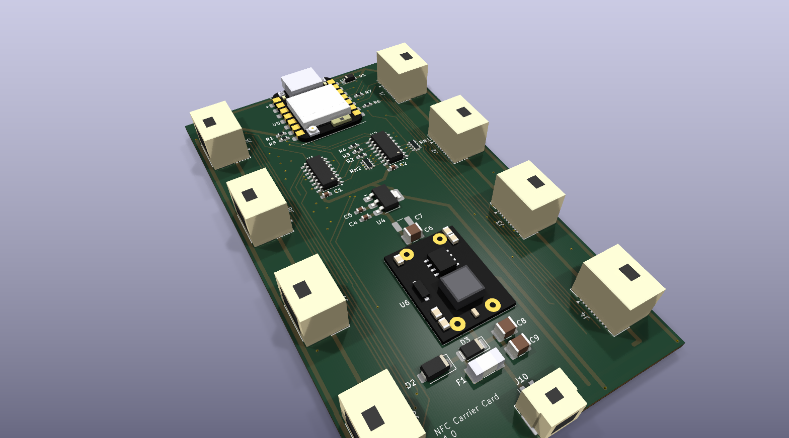
Main components on the Pn5180 carrier
Pn5180 carrier bill of materials (BOM)
35 components, 26 distinct parts — part numbers from the project's BOM.
| Qty | Part | Footprint | Refs |
|---|---|---|---|
| 1 | SN74HC138DR 74HC138 Texas Instruments | SOIC-16_3.9x9.9mm_P1.27mm | U1 |
| 1 | SN74HC151DR 74HC151 Texas Instruments | SOIC-16_3.9x9.9mm_P1.27mm | U2 |
| 1 | TLV1117LV33DCYR Texas Instruments | SOT-223-3_TabPin2 | U4 |
| 1 | XIAO ESP32C6 Seeed Studio | Seeed_XIAO_ESP32C6_SMD | U5 |
| 1 | MP1584EN mini buck module MP1584EN module, fixed 5V Generic (D-SUN style) | MP1584EN_Module_22x17 | U6 |
| 1 | 503148-1090 Bay 0 (CLIK-Mate 2x5) Molex | Molex_CLIK-Mate_503148-1090_2x05-1MP_P1.50mm_Horizontal | J1 |
| 1 | 503148-1090 Bay 1 (CLIK-Mate 2x5) Molex | Molex_CLIK-Mate_503148-1090_2x05-1MP_P1.50mm_Horizontal | J2 |
| 1 | 503148-1090 Bay 2 (CLIK-Mate 2x5) Molex | Molex_CLIK-Mate_503148-1090_2x05-1MP_P1.50mm_Horizontal | J3 |
| 1 | 503148-1090 Bay 3 (CLIK-Mate 2x5) Molex | Molex_CLIK-Mate_503148-1090_2x05-1MP_P1.50mm_Horizontal | J4 |
| 1 | 503148-1090 Bay 4 (CLIK-Mate 2x5) Molex | Molex_CLIK-Mate_503148-1090_2x05-1MP_P1.50mm_Horizontal | J5 |
| 1 | 503148-1090 Bay 5 (CLIK-Mate 2x5) Molex | Molex_CLIK-Mate_503148-1090_2x05-1MP_P1.50mm_Horizontal | J6 |
| 1 | 503148-1090 Bay 6 (CLIK-Mate 2x5) Molex | Molex_CLIK-Mate_503148-1090_2x05-1MP_P1.50mm_Horizontal | J7 |
| 1 | 503148-1090 Bay 7 (CLIK-Mate 2x5) Molex | Molex_CLIK-Mate_503148-1090_2x05-1MP_P1.50mm_Horizontal | J8 |
| 1 | 502494-0270 24V IN (CLIK-Mate 1x2) Molex | Molex_CLIK-Mate_502494-0270_1x02-1MP_P2.00mm_Horizontal | J10 |
| 1 | 0453001.MR 1A Littelfuse | Fuse_Littelfuse-NANO2-451_453 | F1 |
| 1 | PMEG2010AEH Nexperia | D_SOD-123 | D1 |
| 1 | SMAJ28A Littelfuse | D_SMA | D2 |
| 1 | PMEG6030EP Nexperia | D_SOD-128 | D3 |
| 2 | GRM188R71H104KA93D 100nF Murata | C_0603_1608Metric_Pad1.08x0.95mm_HandSolder | C1, C2 |
| 1 | GRM188R61A106KE69D 10uF Murata | C_0603_1608Metric_Pad1.08x0.95mm_HandSolder | C4 |
Show 6 more
| Qty | Part | Footprint | Refs |
|---|---|---|---|
| 1 | GRM188R60J226MEA0D 22uF Murata | C_0603_1608Metric_Pad1.08x0.95mm_HandSolder | C5 |
| 2 | MSASJ32MAB5227MPNDT1 220uF Taiyo Yuden | C_1210_3225Metric_Pad1.33x2.70mm_HandSolder | C6, C7 |
| 2 | GRM32ER71H106KA12L 10uF/50V Murata | C_1210_3225Metric_Pad1.33x2.70mm_HandSolder | C8, C9 |
| 5 | RC0603FR-0710KL 10k Yageo | R_0603_1608Metric_Pad0.98x0.95mm_HandSolder | R1, R2, R3, R4, R5 |
| 2 | RC0603FR-0733RL 33R Yageo | R_0603_1608Metric_Pad0.98x0.95mm_HandSolder | R6, R7 |
| 2 | YC164-FR-07100KL 4x100k Yageo | R_Array_Convex_4x0603 | RN1, RN2 |
Pn5180 carrier design files
The KiCad project lives in the hyiger/pn5180_carrier repository on GitHub; these links point at the commit this page was built from.
- Layoutpn5180_carrier.kicad_pcb
- Schematicpn5180_carrier.kicad_sch
- BOMpn5180_carrier_bom.csv
Pn5180 carrier: common questions
What microcontroller does the Pn5180 carrier use?
The Pn5180 carrier is built around the XIAO ESP32C6, from the ESP32 family.
How big is the Pn5180 carrier PCB?
The Pn5180 carrier measures 62.5 × 106.5 mm, has 2 copper layers and is 1.6 mm thick.
How many components are on the Pn5180 carrier?
35 components, from 26 distinct parts, with part numbers taken from the project's own BOM. The full bill of materials is listed on this page.
Where can I download the Pn5180 carrier design files?
From the hyiger/pn5180_carrier repository on GitHub, which has the KiCad layout, the schematic and the BOM; the links under Design files point to each one.
Can I use the Pn5180 carrier design in my own project?
The repository has no license, so all rights stay with hyiger. Use it as a reference, and ask the author before reusing the design.
Can I test firmware for the Pn5180 carrier without the hardware?
Yes. HardLabs builds a simulation of the board from its netlist and BOM, so you can run and debug ESP32 firmware against it before you order a PCB.
Similar boards
 ESP32
ESP32Open Book Abridged Edition
joeycastillo
85 × 115 mm65 parts2LCC-BY-SA-4.08.1k ESP32
ESP32Badge
atopile
56.3 × 39 mm239 parts4LMIT4.0k ESP32
ESP32Esp32 minimal
36.2 × 26.8 mm20 parts2LMIT4.0k ESP32
ESP32Racer
StuckAtPrototype
36 × 50.2 mm70 parts4LApache-2.03.8k ESP32
ESP32Controller
29 × 74 mm58 parts4LApache-2.03.8k ESP32
ESP32Bitaxe
skot
56.5 × 99.8 mm86 parts4LCERN-OHL-S-2.01.4k