Nlpgen

About the Nlpgen PCB
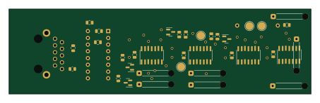
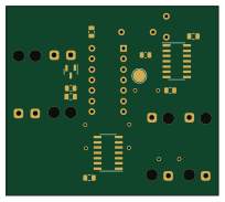
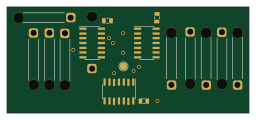
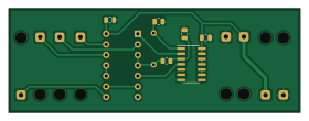
Nlpgen is an open source PCB design by imihajlow, published on GitHub under the GPL-3.0 license. It is a 2-layer board measuring 70 × 25 mm, with 16 components from 12 distinct parts.
Other key parts include the 74HC14 and 74HCT86. By type, the board carries 8 connectors, 4 capacitors, 2 ICs and 2 resistors.
From the project
An Ethernet to SPI converter using 7400-series ICs
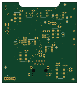
The Nucleo64 shield schematic files are located in sch/shield/.
The firmware for stm32f401 is located in stm32eth-f401/.
The idea is to convert the Manchester-encoded 10BASE-T signal to SPI and use an STM32 MCU to parse it.
A 75C1168 chip is used to convert differential signals to 5V logic levels.
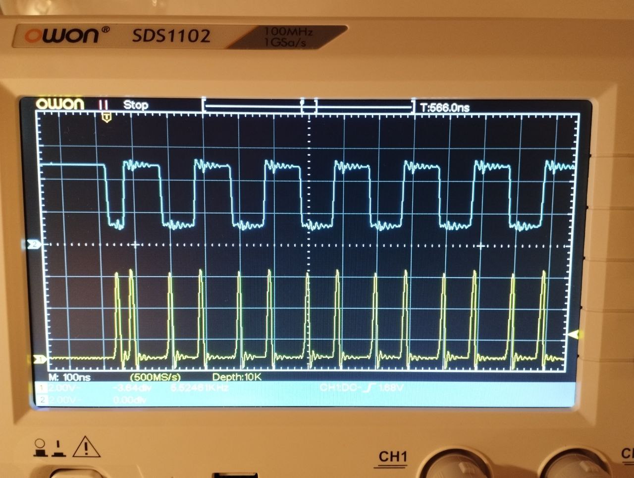
Then, edges are detected using a 74HC86 XOR.
Blue is the input signal, yellow - detected edges.
Main components on the Nlpgen
Nlpgen bill of materials (BOM)
16 components, 12 distinct parts.
| Qty | Part | Footprint | Refs |
|---|---|---|---|
| 1 | 74HC14 | SOIC-14_3.9x8.7mm_P1.27mm | U1 |
| 1 | 74HCT86 | DIP-14_W7.62mm | U2 |
| 2 | vcc | SolderWire-0.5sqmm_1x01_D0.9mm_OD2.3mm_Relief | J1, J7 |
| 2 | gnd | SolderWire-0.5sqmm_1x01_D0.9mm_OD2.3mm_Relief | J2, J8 |
| 1 | nlp_disa | SolderWire-0.5sqmm_1x01_D0.9mm_OD2.3mm_Relief | J3 |
| 1 | sck | SolderWire-0.5sqmm_1x01_D0.9mm_OD2.3mm_Relief | J4 |
| 1 | mosi | SolderWire-0.5sqmm_1x01_D0.9mm_OD2.3mm_Relief | J5 |
| 1 | out | SolderWire-0.5sqmm_1x01_D0.9mm_OD2.3mm_Relief | J6 |
| 3 | 0.1 | C_0805_2012Metric | C1, C2, C4 |
| 1 | 330 | C_0805_2012Metric | C3 |
| 1 | 500k | R_Axial_DIN0204_L3.6mm_D1.6mm_P7.62mm_Horizontal | R1 |
| 1 | 300 | R_0805_2012Metric | R2 |
Nlpgen design files
The KiCad project lives in the imihajlow/ethernet-to-spi repository on GitHub; these links point at the commit this page was built from.
- Layoutsch/nlpgen/nlpgen.kicad_pcb
- Schematicsch/nlpgen/nlpgen.kicad_sch
Nlpgen: common questions
How big is the Nlpgen PCB?
The Nlpgen measures 70 × 25 mm, has 2 copper layers and is 1.6 mm thick.
How many components are on the Nlpgen?
16 components, from 12 distinct parts. The full bill of materials is listed on this page.
Where can I download the Nlpgen design files?
From the imihajlow/ethernet-to-spi repository on GitHub, which has the KiCad layout and the schematic; the links under Design files point to each one.
Can I use the Nlpgen design in my own project?
Yes, under the terms of its GPL-3.0 license, which imihajlow chose for the repository.