
Esp12efplus

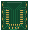
About the Esp12efplus PCB
Esp12efplus is an open source ESP8266 PCB design by jayeye, published on GitHub under the Custom license license. It is a 2-layer board measuring 29.2 × 31.8 mm, with 5 components from 4 distinct parts.
Its main chip is the ESP-12F, from the ESP8266 family. By type, the board carries 2 connectors, 2 capacitors and 1 IC.
From the project
JI's Stuff
Main components on the Esp12efplus
Esp12efplus bill of materials (BOM)
5 components, 4 distinct parts.
| Qty | Part | Footprint | Refs |
|---|---|---|---|
| 1 | ESP-12F | ESP-12E | U1 |
| 2 | Conn_01x12 | PinHeader_1x12_P2.54mm_Vertical | J1, J4 |
| 1 | 100n | C_1206_3216Metric | C1 |
| 1 | 10u | CP_EIA-3528-12_Kemet-T | C2 |
Esp12efplus design files
The KiCad project lives in the jayeye/ji repository on GitHub; these links point at the commit this page was built from.
Esp12efplus: common questions
What microcontroller does the Esp12efplus use?
The Esp12efplus is built around the ESP-12F, from the ESP8266 family.
How big is the Esp12efplus PCB?
The Esp12efplus measures 29.2 × 31.8 mm, has 2 copper layers and is 1.6 mm thick.
How many components are on the Esp12efplus?
5 components, from 4 distinct parts. The full bill of materials is listed on this page.
Where can I download the Esp12efplus design files?
From the jayeye/ji repository on GitHub, which has the KiCad layout; the links under Design files point to each one.
Can I use the Esp12efplus design in my own project?
It is published under Custom license, which limits how it may be reused; read the license before building on it.
Can I test firmware for the Esp12efplus without the hardware?
Yes. HardLabs builds a simulation of the board from its netlist and BOM, so you can run and debug ESP8266 firmware against it before you order a PCB.
More boards in ji
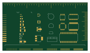
Business Card
88.9 × 50.8 mm42 parts2LCustom license3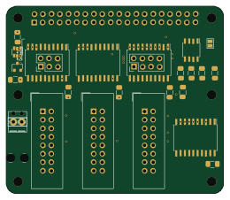 Raspberry Pi
Rpi rgb led matrix nonhat
65 × 56 mm33 parts2LCustom license3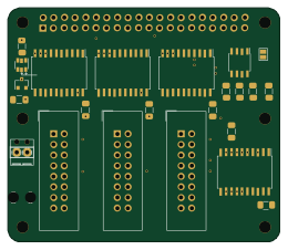 Raspberry Pi
Rpi rgb led matrix hat
65 × 56 mm31 parts2LCustom license3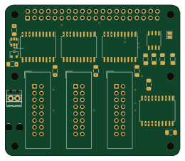 Raspberry Pi
Rpi rgb led matrix hat centeredforprinting
65 × 56 mm31 parts2LCustom license3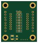
Esp12pogo
33 × 38.1 mm22 parts2LCustom license3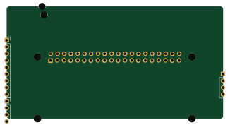
Rpi9341
81.3 × 42.1 mm6 parts2LCustom license3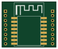 ESP8266
Esp12efs
29.2 × 24.8 mm5 parts2LCustom license3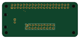 Raspberry Pi
Rpi rgb led matrix zero
65 × 30 mm5 parts2LCustom license3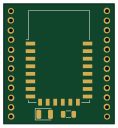 ESP8266
Breakouts
29.2 × 31.8 mm5 parts2LCustom license3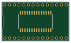
Triple soic ssop
36.1 × 20.8 mm4 parts2LCustom license3
Soic 8 16
10.2 × 10.2 mm3 parts2LCustom license3
Similar boards
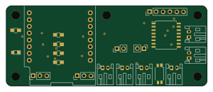 ESP8266
ControllerCircuit
stuartpittaway
75 × 30 mm20 parts2LCC-BY-NC-4.01.1k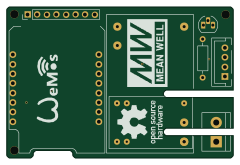 ESP8266
HASwitchPlate
aderusha
60 × 40 mm8 parts2LMIT738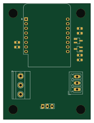 ESP8266
RatGDO-OpenSource-D1Mini-ESP8266
Kaldek
47.8 × 63.3 mm12 parts2LMIT506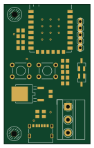 ESP8266
Goatgdo
32.9 × 53.3 mm23 parts2LMIT506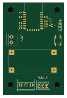 ESP8266
RatGDO-OpenSource-Bare-ESP8266
55 × 82.7 mm20 parts2LMIT506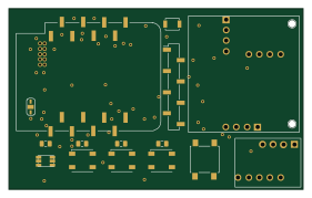 ESP8266
Iaq board
nkitanov
70.1 × 43.2 mm17 parts2LNo license398