
RP2040 Minimal Design Example

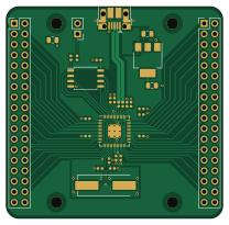
About the RP2040 Minimal Design Example PCB
RP2040 Minimal Design Example is an open source RP2040/RP2350 PCB design by justsem, published on GitHub under the CC-BY-SA-4.0 license. It is a 2-layer board measuring 52 × 51 mm, with 30 components from 14 distinct parts.
Its main chip is the RP2040, from the RP2040/RP2350 family. Other key parts include the NCP1117ST33T3G and W25Q128JVS. By type, the board carries 17 capacitors, 5 resistors, 4 connectors, 3 ICs and 1 crystal.
It belongs with the power & battery, rf & radio and iot & wireless designs in this gallery.
From the project
A GPRS/GNSS/BTLE and LiPo/Li-ion charger integrated Pi Pico on credit-card format.
This is a fully integrated RP2040-based board featuring the following:
GPRS Enabled (with microSIM card format) GNSS (GPS, GLONASS, BEIDOU) BT(LE) Integrated LiPo/Li-ion charging circuit. USB-C (in USB2.0 mode) ports for future proofing. Programmable as if it's a "normal" RPI Pico * Auto-switching power source: In case you connect both the Battery/USB Power and the USB-Program port, the device will automatically switch it's power source to the "PROG" port.
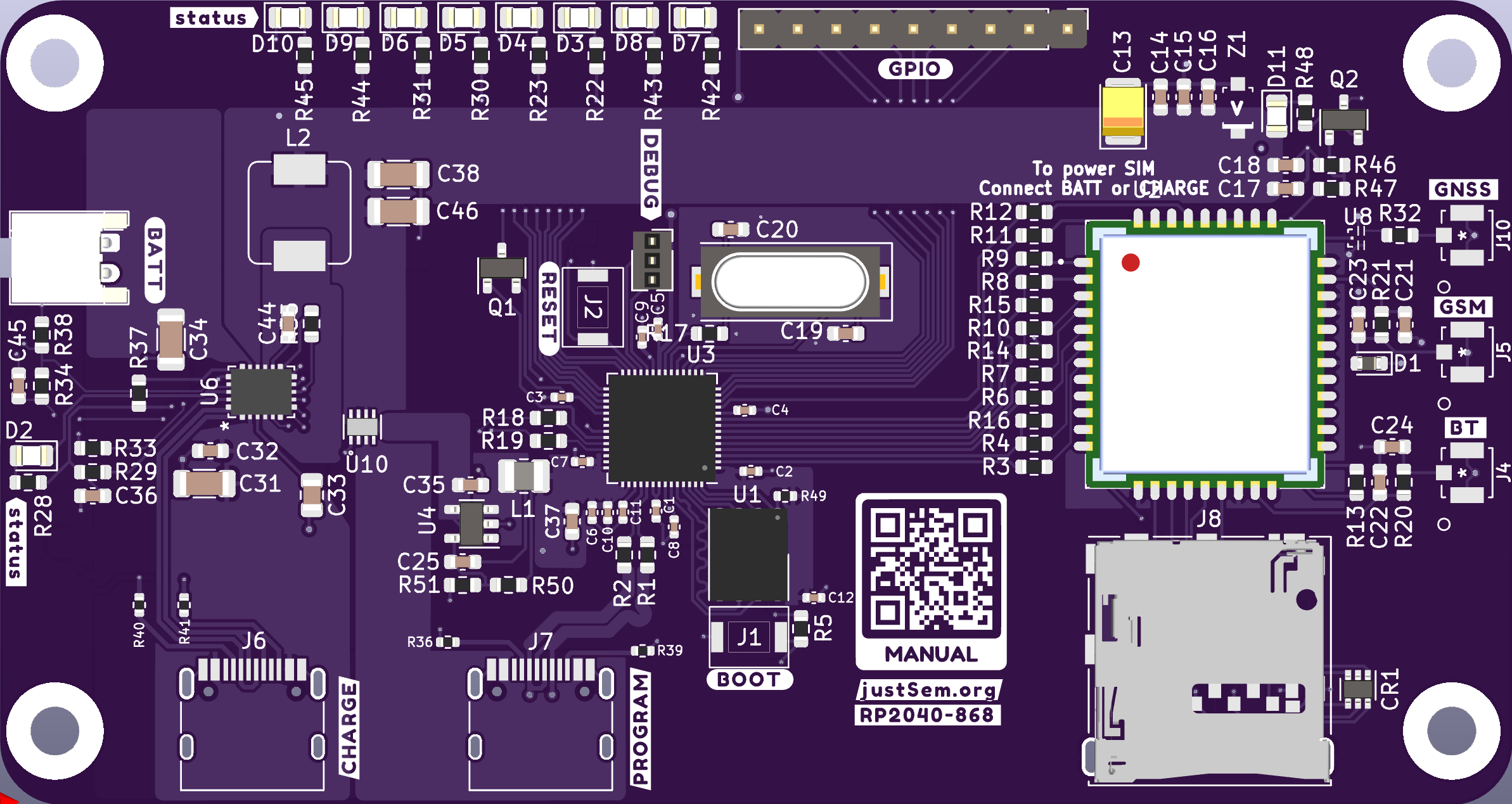
Main components on the RP2040 Minimal Design Example
RP2040 Minimal Design Example bill of materials (BOM)
30 components, 14 distinct parts — part numbers from the project's BOM.
| Qty | Part | Footprint | Refs |
|---|---|---|---|
| 1 | NCP1117ST33T3G NCP1117-3.3_SOT223 ON Semiconductor | SOT-223-3_TabPin2 | U1 |
| 1 | W25Q128JVS Winbond | SOIC-8_5.23x5.23mm_P1.27mm | U2 |
| 1 | RP2040 Raspberry Pi | RP2040-QFN-56 | U3 |
| 1 | ABLS-12.000MHZ-B4-T Abracon | Crystal_SMD_HC49-US | Y1 |
| 1 | 10103594-0001LF USB_B_Micro Amphenol | USB_Micro-B_Amphenol_10103594-0001LF_Horizontal_modified | J1 |
| 1 | TSW-102-23-T-S Conn_01x02 Samtec | PinHeader_1x02_P2.54mm_Vertical | J2 |
| 2 | TSW-118-23-T-D Conn_02x18_Odd_Even Samtec | PinHeader_2x18_P2.54mm_Vertical | J3, J4 |
| 3 | GRM21BR61C106KE15K 10u Murata | C_0805_2012Metric | C1, C4, C17 |
| 2 | GCM1555C1H270JA16D 27p Murata | C_0402_1005Metric | C2, C3 |
| 10 | GRM155R71E104KE14J 100n Murata | C_0402_1005Metric | C5, C6, C7, C9, C11, C12, C13, C14 +2 |
| 2 | GRM155C81A105KA12D 1u Murata | C_0402_1005Metric | C8, C10 |
| 2 | RC0402FR-071KP 1k Yageo | C_0402_1005Metric | R1, R5 |
| 1 | DNF | C_0402_1005Metric | R2 |
| 2 | RC0402FR-0727R4L 27 Yageo | C_0402_1005Metric | R3, R4 |
RP2040 Minimal Design Example design files
The KiCad project lives in the justsem/RP2040-868 repository on GitHub; these links point at the commit this page was built from.
RP2040 Minimal Design Example: common questions
What microcontroller does the RP2040 Minimal Design Example use?
The RP2040 Minimal Design Example is built around the RP2040, from the RP2040/RP2350 family.
How big is the RP2040 Minimal Design Example PCB?
The RP2040 Minimal Design Example measures 52 × 51 mm, has 2 copper layers and is 1 mm thick.
How many components are on the RP2040 Minimal Design Example?
30 components, from 14 distinct parts, with part numbers taken from the project's own BOM. The full bill of materials is listed on this page.
Where can I download the RP2040 Minimal Design Example design files?
From the justsem/RP2040-868 repository on GitHub, which has the KiCad layout, the schematic and the BOM; the links under Design files point to each one.
Can I use the RP2040 Minimal Design Example design in my own project?
Yes, under the terms of its CC-BY-SA-4.0 license, which justsem chose for the repository.
Can I test firmware for the RP2040 Minimal Design Example without the hardware?
Yes. HardLabs builds a simulation of the board from its netlist and BOM, so you can run and debug RP2040/RP2350 firmware against it before you order a PCB.
More boards in RP2040-868
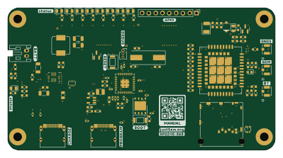
Similar boards
 RP2040/RP2350
Open Book Abridged Edition
joeycastillo
85 × 115 mm29 parts2LCC-BY-SA-4.08.1k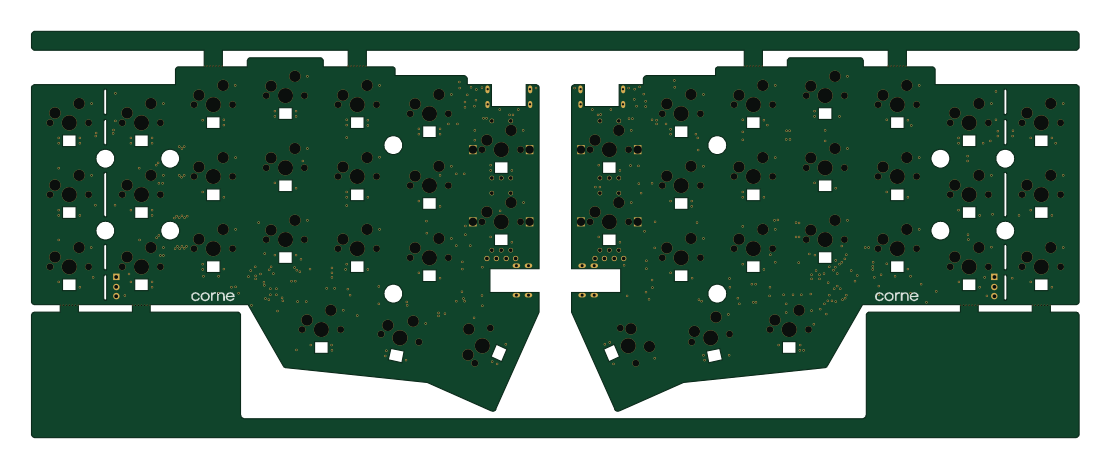 RP2040/RP2350
Corne
foostan
277.2 × 107.5 mm164 parts2LCC-BY-4.07.7k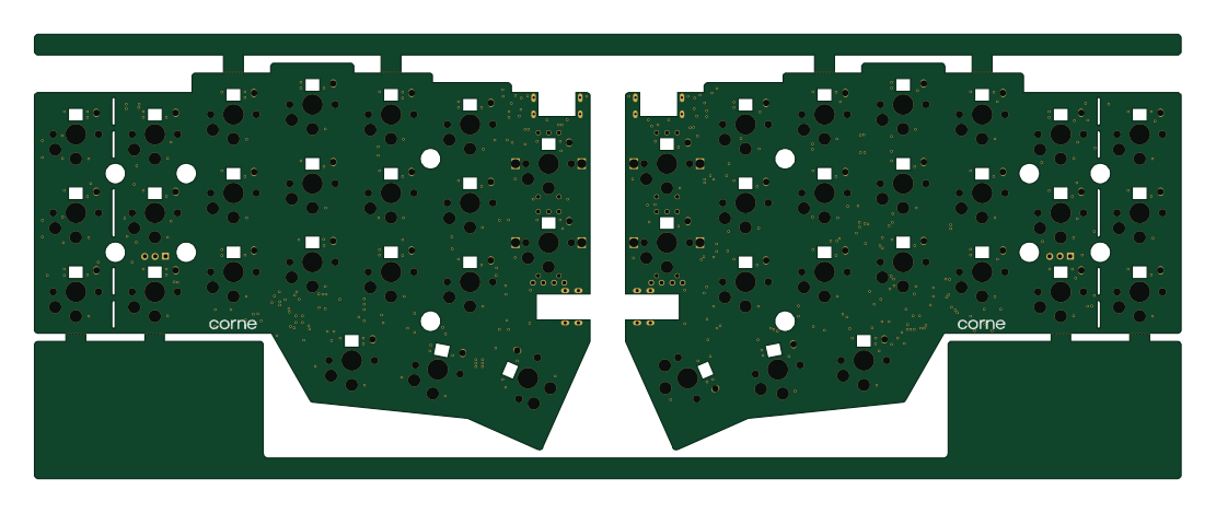 RP2040/RP2350
Corne
277.2 × 107.5 mm164 parts2LCC-BY-4.07.7k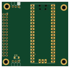 RP2040/RP2350
LogicAnalyzer
gusmanb
57 × 55.2 mm6 parts2LGPL-3.05.0k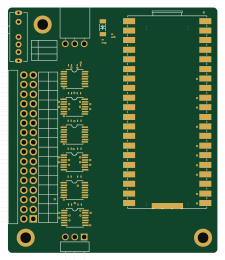 RP2040/RP2350
Jitx design
55.5 × 65 mm26 parts4LGPL-3.05.0k RP2040/RP2350
Pro V2
kata0510
290.1 × 130 mm270 parts2LMIT2.3k