
V2

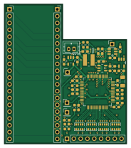
About the V2 PCB
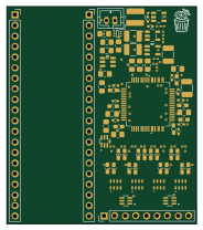
V2 is an open source PCB design by jwmke, published on GitHub. It is a 4-layer board measuring 45.5 × 52 mm, with 64 components from 26 distinct parts.
Other key parts include the ADS1299IPAGR, TPD4E1B06DCKR, LM2664M6, TPS61023DRLR and TPS73233DBVT. By type, the board carries 28 capacitors, 14 resistors, 12 connectors, 9 ICs and 1 inductor.
It belongs with the dev boards & breakouts and power & battery designs in this gallery.
From the project
Open Source 8-channel EEG Pi Pico Shield for <$80
The heart of this PCB is a Texas Instrument's ADS1299, a low noise, 8-Channel, Analog-to-Digital Converter.
Main components on the V2
V2 bill of materials (BOM)
64 components, 26 distinct parts — part numbers from the project's BOM.
| Qty | Part | Footprint | Refs |
|---|---|---|---|
| 1 | ADS1299IPAGR | PAG64_TEX | U1 |
| 3 | TPD4E1B06DCKR | tpd4e1b06dckr | U3, U4, U9 |
| 1 | LM2664M6 | lm266 | U5 |
| 1 | TPS61023DRLR | SOTFL50P160X60-6N | U6 |
| 1 | TPS73233DBVT | 73233 | U7 |
| 1 | TPS72325DBVT | 72325 | U8 |
| 1 | TPS73225DBVR | 73225 | U11 |
| 4 | W2A41C681KAT2A | CAP-ARRAY-SMD_6124-8P-L3.2-W1.6-BL | CN1, CN2, CN3, CN4 |
| 1 | CONN_01X02_PIN Conn_01x02_Pin | JST_PH_B2B-PH-K_1x02_P2.00mm_Vertical | J1 |
| 1 | CONN_01X09_PIN Conn_01x09_Pin | PinHeader_1x09_P2.54mm_Vertical | J2 |
| 2 | CONN_01X20_SOCKET Conn_01x20_Socket | PinSocket_1x20_P2.54mm_Vertical | J3, J4 |
| 4 | Conn_01x01_Pin | PinHeader_1x01_P2.54mm_Vertical | J5, J6, J7, J8 |
| 1 | 1µH | IND_74438357010_WRE | L1 |
| 1 | 1.5NF 1.5nF | C_0603_1608Metric_Pad1.08x0.95mm_HandSolder | C1 |
| 6 | 0.1µF | C_0603_1608Metric_Pad1.08x0.95mm_HandSolder | C2, C6, C8, C11, C15, C16 |
| 4 | 10µF | C_0603_1608Metric_Pad1.08x0.95mm_HandSolder | C3, C18, C19, C22 |
| 9 | 1µF | C_0603_1608Metric_Pad1.08x0.95mm_HandSolder | C4, C5, C9, C10, C12, C14, C17, C27 +1 |
| 1 | 1NF 1nF | C_0603_1608Metric_Pad1.08x0.95mm_HandSolder | C7 |
| 1 | 100µF | C_1206_3216Metric_Pad1.33x1.80mm_HandSolder | C13 |
| 3 | 22µF | C_0603_1608Metric_Pad1.08x0.95mm_HandSolder | C20, C21, C24 |
Show 6 more
| Qty | Part | Footprint | Refs |
|---|---|---|---|
| 3 | 0.01µF | C_0603_1608Metric_Pad1.08x0.95mm_HandSolder | C23, C28, C30 |
| 1 | 1MΩ | R_0603_1608Metric_Pad0.98x0.95mm_HandSolder | R1 |
| 7 | 10kΩ | R_0603_1608Metric_Pad0.98x0.95mm_HandSolder | R2, R3, R6, R7, R8, R9, R10 |
| 1 | 732kΩ | R_0603_1608Metric_Pad0.98x0.95mm_HandSolder | R4 |
| 1 | 100kΩ | R_0603_1608Metric_Pad0.98x0.95mm_HandSolder | R5 |
| 4 | CAY16-103J4LF | RES-ARRAY-SMD_0603-8P-L3.2-W1.6-BL | RN5, RN6, RN7, RN8 |
V2 design files
The KiCad project lives in the jwmke/eeg repository on GitHub; these links point at the commit this page was built from.
- Layoutv2/v2.kicad_pcb
- Schematicv2/v2.kicad_sch
- BOMv2/bom.csv
V2: common questions
How big is the V2 PCB?
The V2 measures 45.5 × 52 mm, has 4 copper layers and is 1.6 mm thick.
How many components are on the V2?
64 components, from 26 distinct parts, with part numbers taken from the project's own BOM. The full bill of materials is listed on this page.
Where can I download the V2 design files?
From the jwmke/eeg repository on GitHub, which has the KiCad layout, the schematic and the BOM; the links under Design files point to each one.
Can I use the V2 design in my own project?
The repository has no license, so all rights stay with jwmke. Use it as a reference, and ask the author before reusing the design.
More boards in eeg
Similar boards
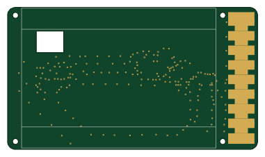
EinkPDA screen
TalismanDesign
95 × 54 mm27 parts2LApache-2.02.0k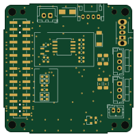
Stack chan
stack-chan
50 × 50 mm33 parts2LApache-2.01.7k
Display Carrier
AxxAxx
35.6 × 58.2 mm5 parts2LGPL-3.01.7k
Eecv breakout
rusefi
140.8 × 53.7 mm9 parts4LGPL-3.01.2k
Breakout 60pin EEC-IV
139.7 × 62.2 mm15 parts2LGPL-3.01.2k
88 Pin Vag Breakout
142 × 58 mm91 parts2LGPL-3.01.2k