
Eda design simulation portfolio


About the Eda design simulation portfolio PCB
Eda design simulation portfolio is an open source PCB design by katherinejenniferhsfeemster, published on GitHub. It is a 2-layer board measuring 50 × 27.5 mm, with 2 components from 2 distinct parts.
Other key parts include the INA128 and OPA2348.
It belongs with the sensors designs in this gallery.
From the project
Code-first EDA portfolio — KiCad, LibrePCB, Ngspice, Qucs-s pipelines for AI research
Tool: KiCad 8 · Language: KiCad S-expression
A clinical-grade differential ECG analog front-end designed for a biosignal dataset pipeline:
- INA128 instrumentation amplifier with gain set by a single Rg resistor. - 1.6 Hz high-pass on each input (DC-block for electrode offset). - 1.06 kHz low-pass anti-alias filter ahead of the ADC buffer. - OPA2348 rail-to-rail op-amp as unity-gain output buffer. - ESD clamps and protection resistors on every patient-connected node.
Main components on the Eda design simulation portfolio
Eda design simulation portfolio bill of materials (BOM)
2 components, 2 distinct parts — part numbers from the project's BOM.
| Qty | Part | Footprint | Refs |
|---|---|---|---|
| 1 | INA128 Texas Instruments | SOIC-8_3.9x4.9mm_P1.27mm | U1 |
| 1 | OPA2348 Texas Instruments | SOIC-8_3.9x4.9mm_P1.27mm | U2 |
Eda design simulation portfolio design files
The KiCad project lives in the katherinejenniferhsfeemster/eda-design-simulation-portfolio repository on GitHub; these links point at the commit this page was built from.
Eda design simulation portfolio: common questions
How big is the Eda design simulation portfolio PCB?
The Eda design simulation portfolio measures 50 × 27.5 mm, has 2 copper layers and is 1.6 mm thick.
How many components are on the Eda design simulation portfolio?
2 components, from 2 distinct parts, with part numbers taken from the project's own BOM. The full bill of materials is listed on this page.
Where can I download the Eda design simulation portfolio design files?
From the katherinejenniferhsfeemster/eda-design-simulation-portfolio repository on GitHub, which has the KiCad layout, the schematic and the BOM; the links under Design files point to each one.
Can I use the Eda design simulation portfolio design in my own project?
The repository has no license, so all rights stay with katherinejenniferhsfeemster. Use it as a reference, and ask the author before reusing the design.
Similar boards

Sensors
StuckAtPrototype
15.2 × 9 mm14 parts4LApache-2.03.8k
Microphone
Mentra-Community
5.5 × 6.1 mm6 parts2LMIT1.2k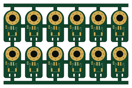
TemperaturePCB PANEL
stuartpittaway
116 × 75.5 mm178 parts2LCC-BY-NC-4.01.1k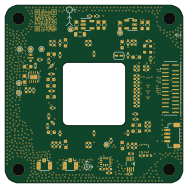
FourThirdsEye
will127534
47 × 47 mm106 parts4LMIT377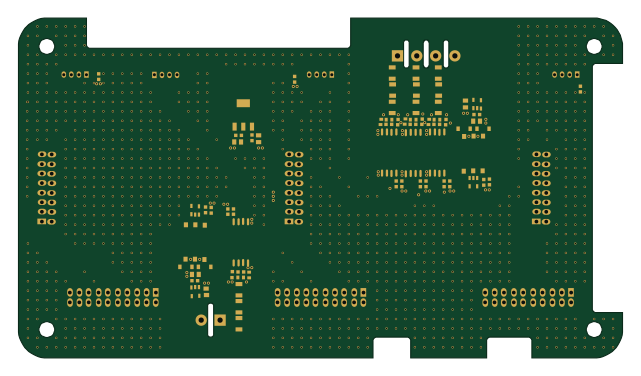
VESC Controller
paltatech
160 × 90 mm908 parts2LNo license354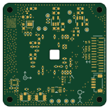
OneInchEye
39 × 39 mm79 parts4LMIT346