
Ssla

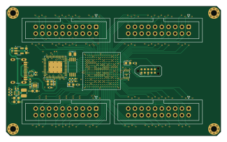
About the Ssla PCB
Ssla is an open source FPGA PCB design by korken89, published on GitHub. It is a 4-layer board measuring 81 × 49 mm, with 214 components from 29 distinct parts.
Its main chip is the ECP5U_25_CABGA256, from the FPGA family. Other key parts include the TLV75533PDRV, AP2127K-2.5, BL24C256A, USBLC6-2P6 and CY7C68013A-56LTX. By type, the board carries 83 resistors, 66 diodes, 49 capacitors, 8 ICs, 5 connectors and 2 inductors.
Main components on the Ssla
Ssla bill of materials (BOM)
214 components, 29 distinct parts — part numbers from the project's BOM.
| Qty | Part | Footprint | Refs |
|---|---|---|---|
| 1 | TLV75533PDRV | WSON-6-1EP_2x2mm_P0.65mm_EP1x1.6mm | U1 |
| 1 | AP2127K-2.5 | SOT-23-5 | U2 |
| 1 | BL24C256A | TSSOP-8_4.4x3mm_P0.65mm | U3 |
| 1 | USBLC6-2P6 | SOT-666 | U4 |
| 1 | CY7C68013A-56LTX | QFN-56-1EP_8x8mm_P0.5mm_EP4.5x5.2mm | U5 |
| 1 | ECP5U_25_CABGA256 | BGA-256_14.0x14.0mm_Layout16x16_P0.8mm_Ball0.45mm_Pad0.32mm_NSMD | U6 |
| 1 | W25Q16JVUXIQ | Winbond_USON-8-1EP_3x2mm_P0.5mm_EP0.2x1.6mm | U7 |
| 1 | TPS62A01ADRLR | SOT-563 | U8 |
| 1 | C2689430 24 MHz | Crystal_SMD_2016-4Pin_2.0x1.6mm | Y1 |
| 1 | USB_C_RECEPTACLE_USB2.0_14P USB_C_Receptacle_USB2.0_14P | USB_C_Receptacle_GCT_USB4105-xx-A_16P_TopMnt_Horizontal | J1 |
| 4 | CONN_02X10_ODD_EVEN Conn_02x10_Odd_Even | IDC-Header_2x10_P2.54mm_Vertical | J2, J3, J4, J5 |
| 64 | C96512 D_TVS_Small | D_SOD-923 | D1, D2, D3, D4, D5, D6, D7, D8 +56 |
| 2 | LED_Small | LED_0603_1608Metric | D65, D66 |
| 1 | C491490 FerriteBead_Small | R_0402_1005Metric | FB1 |
| 1 | 1.5U 1.5u | L_1008_2520Metric | L1 |
| 11 | 10N 10n | C_0402_1005Metric | C1, C5, C9, C10, C14, C17, C37, C39 +3 |
| 23 | 0.1U 0.1u | C_0402_1005Metric | C2, C4, C6, C7, C11, C12, C13, C15 +15 |
| 8 | 4.7U 4.7u | C_0402_1005Metric | C3, C8, C23, C24, C46, C47, C48, C49 |
| 2 | 12P 12p | C_0402_1005Metric | C19, C20 |
| 4 | 10U 10u | C_0603_1608Metric | C28, C31, C33, C34 |
Show 9 more
| Qty | Part | Footprint | Refs |
|---|---|---|---|
| 1 | 27P 27p | C_0402_1005Metric | C32 |
| 2 | 5.1K 5.1k | R_0402_1005Metric | R1, R2 |
| 6 | 1k | R_0402_1005Metric | R3, R9, R10, R43, R44, R83 |
| 1 | 0 | R_0805_2012Metric | R4 |
| 2 | 2.2K 2.2k | R_0402_1005Metric | R5, R7 |
| 3 | 100K 100k | R_0402_1005Metric | R6, R8, R82 |
| 64 | 100 | R_0402_1005Metric | R11, R12, R13, R14, R15, R16, R17, R18 +56 |
| 4 | 10K 10k | R_0402_1005Metric | R45, R78, R79, R80 |
| 1 | 82K 82k | R_0402_1005Metric | R81 |
Ssla design files
The KiCad project lives in the korken89/ssla repository on GitHub; these links point at the commit this page was built from.
- Layoutssla.kicad_pcb
- Schematicssla.kicad_sch
- BOMproduction/bom.csv
Ssla: common questions
What microcontroller does the Ssla use?
The Ssla is built around the ECP5U_25_CABGA256, from the FPGA family.
How big is the Ssla PCB?
The Ssla measures 81 × 49 mm, has 4 copper layers and is 1.6 mm thick.
How many components are on the Ssla?
214 components, from 29 distinct parts, with part numbers taken from the project's own BOM. The full bill of materials is listed on this page.
Where can I download the Ssla design files?
From the korken89/ssla repository on GitHub, which has the KiCad layout, the schematic and the BOM; the links under Design files point to each one.
Can I use the Ssla design in my own project?
The repository has no license, so all rights stay with korken89. Use it as a reference, and ask the author before reusing the design.
Can I test firmware for the Ssla without the hardware?
Yes. HardLabs builds a simulation of the board from its netlist and BOM, so you can run and debug FPGA firmware against it before you order a PCB.
Similar boards
 FPGA
Base board
GlasgowEmbedded
80 × 49 mm222 parts4L0BSD2.2k FPGA
Thunderscope Rev5.3
EEVengers
122.5 × 103.5 mm817 parts6LMIT1.3k FPGA
Usb sniffer
ataradov
58.2 × 38.1 mm86 parts2LBSD-3-Clause1.3k FPGA
Tomu, I'm
theacodes
13 × 9.4 mm40 parts4LMIT1.1k FPGA
Icepi zero
cheyao
65 × 30 mm143 parts4LSHL-2.1865 FPGA
Gcvideo
ikorb
49 × 30 mm44 parts4LNo license765