
Hello-My-Name-Is-PCB-Badge

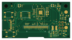
About the Hello-My-Name-Is-PCB-Badge
Hello-My-Name-Is-PCB-Badge is an open source RP2040/RP2350 PCB design by MitchellStride, published on GitHub under the CERN-OHL-S-2.0 license. It is a 2-layer board measuring 59 × 31.5 mm, with 75 components from 33 distinct parts.
Its main chip is the RP2040, from the RP2040/RP2350 family. Other key parts include the RT9080-33GJ5, TPS61040DBV and W25Q64JV. By type, the board carries 28 capacitors, 20 resistors, 5 switches, 5 diodes, 4 ICs and 3 connectors.
It belongs with the wearables and power & battery designs in this gallery.
From the project
#badgelife
This #Badgelife PCB was created to test some circuits for future art PCBs. It also served as a small project to bring to local hardware meetups. Partial assembly was done at JLCPCB.
- I saw someone else's design online using an RGB LED running at 3.3V (below spec). I tried to replicate it, and the LEDs were very flaky and worked intermittently. Experiment failed 😢. - AA boost converter not yet tested; currently using USB power only.
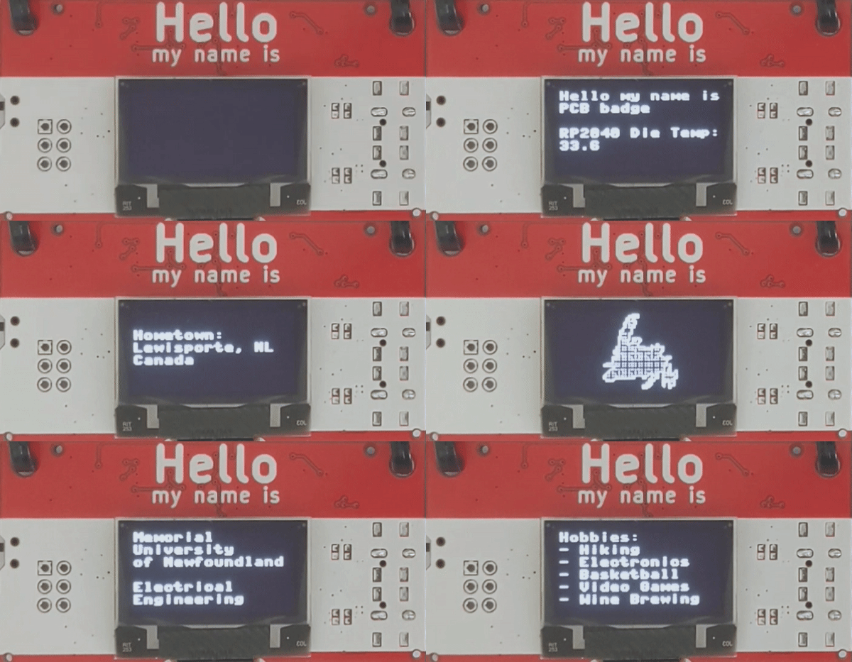
Main components on the Hello-My-Name-Is-PCB-Badge
Hello-My-Name-Is-PCB-Badge bill of materials (BOM)
75 components, 33 distinct parts.
| Qty | Part | Footprint | Refs |
|---|---|---|---|
| 1 | RT9080-33GJ5 | SOT-23-5 | U1 |
| 1 | TPS61040DBV | SOT-23-5 | U2 |
| 1 | RP2040 | QFN-56_EP_7x7_Pitch0.4mm | U3 |
| 1 | W25Q64JV | SOIC-8W_5.3x5.3mm_P1.27mm | U4 |
| 1 | AO3401A | SOT-23 | Q1 |
| 1 | AO3400A | SOT-23 | Q2 |
| 1 | XYDBPCNANF-12MHZ | Crystal_SMD_2520-4Pin_2.5x2.0mm | Y1 |
| 1 | USB_C_Receptacle_USB2.0 | USB-C-16p | J1 |
| 1 | OLED | OLED-128O064D | J2 |
| 1 | SAO 2x3 IDC | Badgelife-SAOv169-BADGE-2x3 | P1 |
| 1 | AAx2 | BatteryHolder_MPD_BC2AAPC_2xAA_mod-SMD | BT1 |
| 1 | 24V 500mA PTC | Fuse_0805_2012Metric | F1 |
| 4 | Tooling_Hole_JLC | JLC_Tooling_Hole | H1, H2, H3, H4 |
| 1 | SSSS811101 | SSSS811101 | SW1 |
| 4 | TS-1187A-B-A-B | SW_SPST_TL3342 | SW2, SW3, SW4, SW5 |
| 4 | WS2812B-2020 | WS2812B-2020 | D1, D2, D4, D5 |
| 1 | 1N5819WS | D_SOD-323 | D3 |
| 1 | 3.3u | L_Bourns-SRN4018 | L1 |
| 13 | 1u | C_0402_1005Metric | C1, C5, C6, C8, C9, C12, C22, C23 +5 |
| 4 | 4.7u | C_0402_1005Metric | C2, C3, C4, C11 |
Show 13 more
| Qty | Part | Footprint | Refs |
|---|---|---|---|
| 1 | 2.2u | C_0402_1005Metric | C7 |
| 1 | 3.3p | C_0402_1005Metric | C10 |
| 7 | 0.1u | C_0402_1005Metric | C13, C14, C15, C16, C17, C18, C19 |
| 2 | 12p | C_0402_1005Metric | C20, C21 |
| 7 | 10k | R_0402_1005Metric | R1, R2, R13, R14, R15, R16, R19 |
| 2 | 56k | R_0402_1005Metric | R3, R4 |
| 3 | 1k | R_0402_1005Metric | R5, R6, R20 |
| 1 | 200k | R_0402_1005Metric | R7 |
| 1 | 51k | R_0402_1005Metric | R8 |
| 1 | 150k | R_0402_1005Metric | R9 |
| 1 | 330k | R_0402_1005Metric | R10 |
| 2 | 4.7k | R_0402_1005Metric | R11, R12 |
| 2 | 22 | R_0402_1005Metric | R17, R18 |
Hello-My-Name-Is-PCB-Badge design files
The KiCad project lives in the MitchellStride/Hello-My-Name-Is-PCB-Badge repository on GitHub; these links point at the commit this page was built from.
Hello-My-Name-Is-PCB-Badge: common questions
What microcontroller does the Hello-My-Name-Is-PCB-Badge use?
The Hello-My-Name-Is-PCB-Badge is built around the RP2040, from the RP2040/RP2350 family.
How big is the Hello-My-Name-Is-PCB-Badge?
The Hello-My-Name-Is-PCB-Badge measures 59 × 31.5 mm, has 2 copper layers and is 1.6 mm thick.
How many components are on the Hello-My-Name-Is-PCB-Badge?
75 components, from 33 distinct parts. The full bill of materials is listed on this page.
Where can I download the Hello-My-Name-Is-PCB-Badge design files?
From the MitchellStride/Hello-My-Name-Is-PCB-Badge repository on GitHub, which has the KiCad layout and the schematic; the links under Design files point to each one.
Can I use the Hello-My-Name-Is-PCB-Badge design in my own project?
Yes, under the terms of its CERN-OHL-S-2.0 license, which MitchellStride chose for the repository.
Can I test firmware for the Hello-My-Name-Is-PCB-Badge without the hardware?
Yes. HardLabs builds a simulation of the board from its netlist and BOM, so you can run and debug RP2040/RP2350 firmware against it before you order a PCB.
Similar boards
 RP2040/RP2350
Open Book Abridged Edition
joeycastillo
85 × 115 mm29 parts2LCC-BY-SA-4.08.1k RP2040/RP2350
Corne
foostan
277.2 × 107.5 mm164 parts2LCC-BY-4.07.7k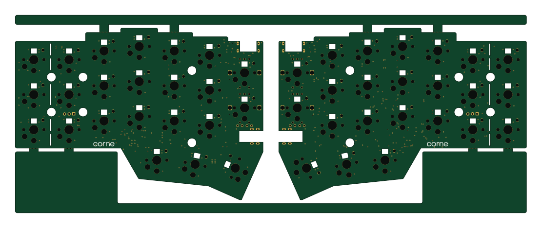 RP2040/RP2350
Corne
277.2 × 107.5 mm164 parts2LCC-BY-4.07.7k RP2040/RP2350
Jitx design
gusmanb
55.5 × 65 mm26 parts4LGPL-3.05.0k RP2040/RP2350
LogicAnalyzer
57 × 55.2 mm6 parts2LGPL-3.05.0k RP2040/RP2350
Main
google
98 × 71 mm102 parts2LApache-2.02.9k