
Atonceplus

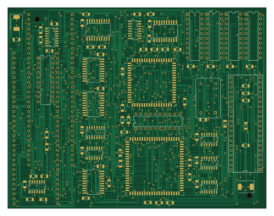
About the Atonceplus PCB
Atonceplus is an open source PCB design by na103, published on GitHub under the CC-BY-NC-4.0 license. It is a 4-layer board measuring 135 × 105 mm, with 85 components from 26 distinct parts.
Other key parts include the N80C286-16, 80C287, 74LS08, 74HCT374 and GAL16V8. By type, the board carries 30 capacitors, 30 resistors, 22 ICs, 2 connectors and 1 transistor.
It belongs with the retro computing designs in this gallery.
From the project
Amiga 500 PC AT 286 emulator board
Amiga Dueottosei (Italian for "two-eight-six") is a clone of the Vortex ATonce Plus, a PC AT Emulator board for the Amiga 500.
Fully compatible 16 MHz PC/AT emulator CMOS 80C286-16 CPU chip 512 KB onboard RAM Socket for optional 80C287-12 math coprocessor Fully AT compatible ROM/BIOS Full 640 KB base memory as minimum standard configuration Ability to address additional FAST RAM as either Extended or Expanded Memory Runs unrestricted in '286 Protected Mode Supports Microsoft Windows 3.0 and Windows 3.1 Emulates EGA and VGA monochrome graphics, CGA 16-color graphics, Hercules, Olivetti and…
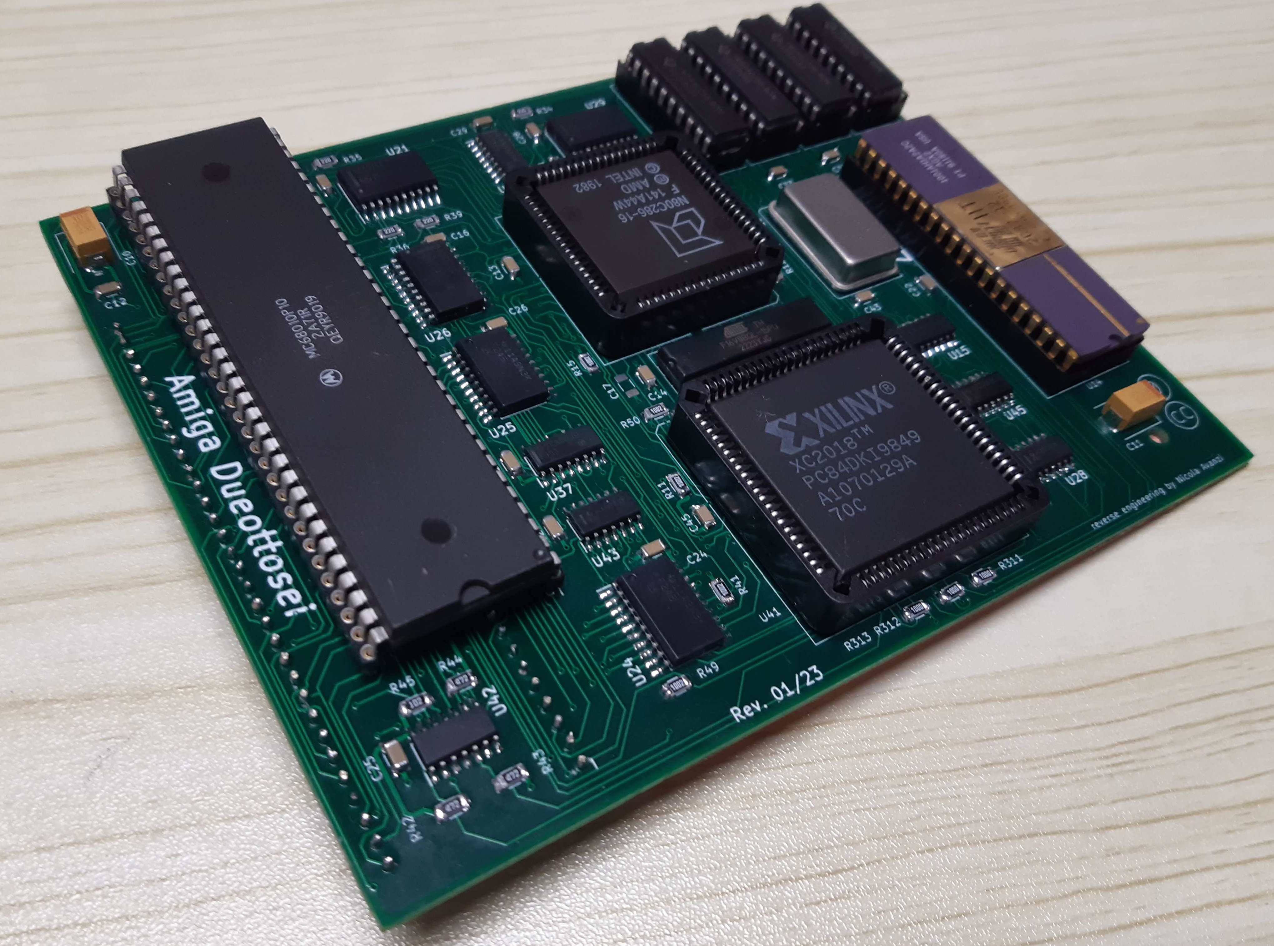
Main components on the Atonceplus
Atonceplus bill of materials (BOM)
85 components, 26 distinct parts.
| Qty | Part | Footprint | Refs |
|---|---|---|---|
| 1 | N80C286-16 | PLCC-68 | U13 |
| 1 | 80C287 | DIP-40_W15.24mm_Socket | U14 |
| 1 | 74LS08 | SOIC127P600X175-14N | U15 |
| 3 | 74HCT374 | SOIC127P1030X265-20N | U21, U26, U29 |
| 2 | GAL16V8 | DIP-20_W7.62mm | U22, U44 |
| 2 | SN74F245DWR | SOIC127P1030X265-20N | U24, U25 |
| 1 | SN74F86D | SOIC127P600X175-14N | U28 |
| 4 | TMS44C256-80 | DIP-20_W7.62mm | U31, U32, U33, U34 |
| 2 | SN74F157AD | SOIC127P600X175-16N | U35, U36 |
| 1 | SN74F153D | SOIC127P600X175-16N | U37 |
| 1 | XC2018-PC84 | PLCC-84 | U41 |
| 1 | SN74F125D | SOIC127P600X175-14N | U42 |
| 1 | SN74F00D | SOIC127P600X175-14N | U43 |
| 1 | SN74F260D | SOIC127P600X175-14N | U45 |
| 1 | 32MHz | Oscillator_DIP-14 | Q1 |
| 1 | Amiga board 68k socket | DIPS2286W51P254L8128H419Q64N | J1 |
| 1 | Motorola 68k CPU | DIPS2286W51P254L8128H419Q64N | J2 |
| 2 | 100uF | CP_EIA-7361-438_AVX-U | C10, C11 |
| 27 | 100nF | C_1206_3216Metric | C12, C13, C14, C15, C16, C21, C22, C23 +19 |
| 1 | empty | C_1206_3216Metric | C17 |
Show 6 more
| Qty | Part | Footprint | Refs |
|---|---|---|---|
| 10 | 10K | R_1206_3216Metric | R11, R12, R13, R14, R15, R16, R17, R41 +2 |
| 9 | 22 | R_1206_3216Metric | R31, R32, R33, R34, R35, R36, R37, R38 +1 |
| 5 | 4.7K | R_1206_3216Metric | R42, R43, R44, R47, R48 |
| 2 | 1K | R_1206_3216Metric | R45, R46 |
| 1 | 2.2K | R_1206_3216Metric | R110 |
| 3 | 100 | R_1206_3216Metric | R311, R312, R313 |
Atonceplus design files
The KiCad project lives in the na103/Dueottosei repository on GitHub; these links point at the commit this page was built from.
Atonceplus: common questions
How big is the Atonceplus PCB?
The Atonceplus measures 135 × 105 mm, has 4 copper layers and is 1.6 mm thick.
How many components are on the Atonceplus?
85 components, from 26 distinct parts. The full bill of materials is listed on this page.
Where can I download the Atonceplus design files?
From the na103/Dueottosei repository on GitHub, which has the KiCad layout; the links under Design files point to each one.
Can I use the Atonceplus design in my own project?
It is published under CC-BY-NC-4.0, which limits how it may be reused; read the license before building on it.
More boards in Dueottosei
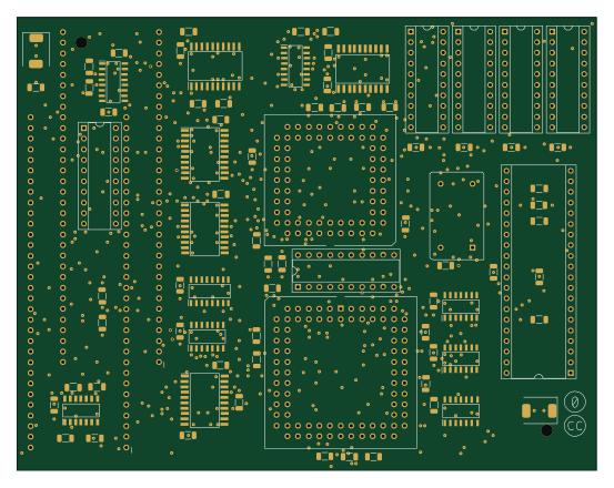
Similar boards
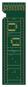
Amiga External
hoglet67
21.9 × 76.7 mm6 parts2LGPL-3.01.0k
Atari pickup
26.4 × 53.9 mm7 parts2LGPL-3.01.0k
Deniseadapter
26.7 × 62.2 mm16 parts2LGPL-3.01.0k
Analog
53.9 × 23.2 mm33 parts2LGPL-3.01.0k
Rgb to hdmi
77 × 97 mm67 parts2LGPL-3.01.0k
Buffer
53.9 × 23.2 mm13 parts2LGPL-3.01.0k