
My devboard-

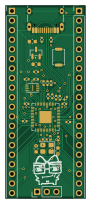
About the My devboard- PCB
My devboard- is an open source RP2040/RP2350 PCB design by Nitish5196, published on GitHub. It is a 2-layer board measuring 21 × 51 mm, with 33 components from 16 distinct parts.
Its main chip is the RP2040, from the RP2040/RP2350 family. Other key parts include the MCP1700T-3302E/TT and W25Q16JVZPIQ. By type, the board carries 17 capacitors, 7 resistors, 4 connectors, 3 ICs, 1 crystal and 1 switch.
It belongs with the dev boards & breakouts designs in this gallery.
Main components on the My devboard-
My devboard- bill of materials (BOM)
33 components, 16 distinct parts — part numbers from the project's BOM.
| Qty | Part | Footprint | Refs |
|---|---|---|---|
| 1 | RP2040 | QFN-56-1EP_7x7mm_P0.4mm_EP3.2x3.2mm | U1 |
| 1 | MCP1700T-3302E/TT MCP1700x-330xxTT | SOT-23 | U2 |
| 1 | W25Q16JVZPIQ | Winbond_USON-8-1EP_3x2mm_P0.5mm_EP0.2x1.6mm | U3 |
| 1 | ABM8G-12.000MHZ-18-D2Y-T 12 MHz | Crystal_SMD_3225-4Pin_3.2x2.5mm | Y1 |
| 1 | TYPE-C-31-M-12 USB_C_Receptacle_USB2.0_14P | USB_C_Receptacle_HRO_TYPE-C-31-M-12 | J1 |
| 2 | 61302011121 Conn_01x20 | PinHeader_1x20_P2.54mm_Vertical | J2, J3 |
| 1 | 61300311121 Conn_01x03 | PinHeader_1x03_P2.54mm_Vertical | J4 |
| 1 | PTS645SM43SMTR92LFS SW_Push | SW_Push_SPST_NO_Alps_SKRK | SW1 |
| 2 | CL05A105KO5NNNC 1uF | C_0402_1005Metric | C1, C10 |
| 11 | CL05B104KO5NNNC 0.1uF | C_0402_1005Metric | C2, C3, C4, C5, C6, C7, C8, C9 +3 |
| 2 | CL10A106KP8NNNC 10uF | C_0603_1608Metric | C13, C14 |
| 2 | CL10C330JB8NNNC 33pF | C_0603_1608Metric | C15, C16 |
| 2 | RC0402JR-075K1L 5.1K | R_0402_1005Metric | R1, R2 |
| 2 | RC0402JR-0727RL 27 | R_0402_1005Metric | R3, R4 |
| 2 | RC0402JR-071KL 1K | R_0402_1005Metric | R5, R7 |
| 1 | RC0402JR-0710KL 10K | R_0402_1005Metric | R6 |
My devboard- design files
The KiCad project lives in the Nitish5196/my-devboard- repository on GitHub; these links point at the commit this page was built from.
My devboard-: common questions
What microcontroller does the My devboard- use?
The My devboard- is built around the RP2040, from the RP2040/RP2350 family.
How big is the My devboard- PCB?
The My devboard- measures 21 × 51 mm, has 2 copper layers and is 1.6 mm thick.
How many components are on the My devboard-?
33 components, from 16 distinct parts, with part numbers taken from the project's own BOM. The full bill of materials is listed on this page.
Where can I download the My devboard- design files?
From the Nitish5196/my-devboard- repository on GitHub, which has the KiCad layout, the schematic and the BOM; the links under Design files point to each one.
Can I use the My devboard- design in my own project?
The repository has no license, so all rights stay with Nitish5196. Use it as a reference, and ask the author before reusing the design.
Can I test firmware for the My devboard- without the hardware?
Yes. HardLabs builds a simulation of the board from its netlist and BOM, so you can run and debug RP2040/RP2350 firmware against it before you order a PCB.
Similar boards
 RP2040/RP2350
Open Book Abridged Edition
joeycastillo
85 × 115 mm29 parts2LCC-BY-SA-4.08.1k RP2040/RP2350
Corne
foostan
277.2 × 107.5 mm164 parts2LCC-BY-4.07.7k RP2040/RP2350
Corne
277.2 × 107.5 mm164 parts2LCC-BY-4.07.7k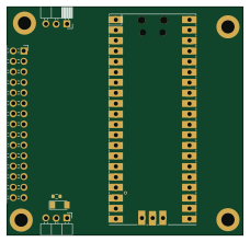 RP2040/RP2350
LogicAnalyzer
gusmanb
57 × 55.2 mm6 parts2LGPL-3.05.0k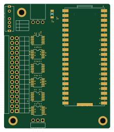 RP2040/RP2350
Jitx design
55.5 × 65 mm26 parts4LGPL-3.05.0k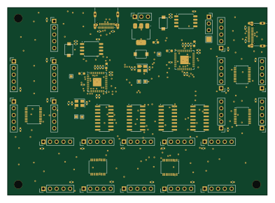 RP2040/RP2350
Main
google
98 × 71 mm102 parts2LApache-2.02.9k