
Button grid

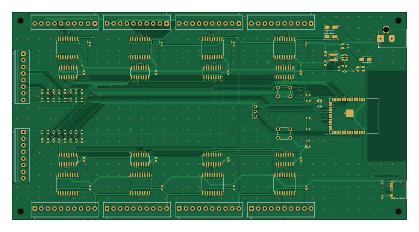
About the Button grid PCB
Button grid is an open source ESP32 PCB design by paulsonnentag, published on GitHub. It is a 2-layer board measuring 208 × 110 mm, with 104 components from 26 distinct parts.
Its main chip is the ESP32-S3-WROOM-1-N8, from the ESP32 family. Other key parts include the TPS54202H, 74HC595 and ULN2803A. By type, the board carries 40 resistors, 26 capacitors, 18 ICs, 13 connectors, 4 diodes and 2 switches.
It belongs with the power & battery designs in this gallery.
From the project
An ESP32-S3 controller board for an 8×8 button matrix with 64 individually switched 12 V LEDs. It's designed in KiCad 9 and made to be ordered from JLCPCB.
An ESP32-S3 controller board for an 8×8 button matrix with 64 individually switched 12 V LEDs. It's designed in KiCad 9 and made to be ordered from JLCPCB.
Site with the design viewer, test results and JLCPCB downloads: GitHub Pages for this repo, built by .github/workflows/pages.yml.
- LED terminals J11–J18 (10-pole, 3.5 mm pitch, along the top and bottom edges). Pins 1–8 take the cathode (−) wire of 8 LEDs. Pins 9–10 are +12 V for the anode (+) wires. Each LED must keep its own series resistor. Twist or daisy-chain the + wires of a bank so that at most 2 wires go into one screw. Bank 1…
Main components on the Button grid
Button grid bill of materials (BOM)
104 components, 26 distinct parts.
| Qty | Part | Footprint | Refs |
|---|---|---|---|
| 1 | ESP32-S3-WROOM-1-N8 | ESP32-S3-WROOM-1 | U1 |
| 1 | TPS54202H | TSOT-23-6 | U2 |
| 8 | 74HC595 | SOIC-16_3.9x9.9mm_P1.27mm | U11, U12, U13, U14, U15, U16, U17, U18 |
| 8 | ULN2803A | SOIC-18W_7.5x11.6mm_P1.27mm | U21, U22, U23, U24, U25, U26, U27, U28 |
| 1 | 12V DC | BarrelJack_Horizontal | J1 |
| 1 | USB-C | USB_C_Receptacle_HRO_TYPE-C-31-M-12 | J2 |
| 1 | ROWS | TerminalBlock_Phoenix_PT-1,5-8-3.5-H_1x08_P3.50mm_Horizontal | J3 |
| 1 | COLS | TerminalBlock_Phoenix_PT-1,5-8-3.5-H_1x08_P3.50mm_Horizontal | J4 |
| 1 | UART | PinHeader_1x03_P2.54mm_Vertical | J5 |
| 8 | LEDs | TerminalBlock_Phoenix_PT-1,5-10-3.5-H_1x10_P3.50mm_Horizontal | J11, J12, J13, J14, J15, J16, J17, J18 |
| 1 | RESET | SW_PUSH_6mm | SW1 |
| 1 | BOOT | SW_PUSH_6mm | SW2 |
| 1 | SS54 | D_SMA | D1 |
| 2 | SS34 | D_SMA | D2, D3 |
| 1 | status | LED_0603_1608Metric | D4 |
| 1 | 10uH | L_Sunlord_SWPA4030S | L1 |
| 4 | 10uF 25V | C_0805_2012Metric | C1, C2, C3, C9 |
| 19 | 100nF | C_0603_1608Metric | C4, C5, C10, C11, C12, C13, C14, C15 +11 |
| 2 | 22uF | C_0805_2012Metric | C6, C7 |
| 1 | 1uF | C_0603_1608Metric | C8 |
Show 6 more
| Qty | Part | Footprint | Refs |
|---|---|---|---|
| 1 | 100k | R_0603_1608Metric | R1 |
| 17 | 22k | R_0603_1608Metric | R2, R30, R31, R32, R33, R34, R35, R36 +9 |
| 3 | 10k | R_0603_1608Metric | R3, R4, R5 |
| 1 | 1k | R_0603_1608Metric | R6 |
| 2 | 5.1k | R_0603_1608Metric | R7, R8 |
| 16 | 100 | R_0603_1608Metric | R10, R11, R12, R13, R14, R15, R16, R17 +8 |
Button grid design files
The KiCad project lives in the paulsonnentag/button-grid repository on GitHub; these links point at the commit this page was built from.
- Layouthardware/button-grid.kicad_pcb
- Schematichardware/button-grid.kicad_sch
Button grid: common questions
What microcontroller does the Button grid use?
The Button grid is built around the ESP32-S3-WROOM-1-N8, from the ESP32 family.
How big is the Button grid PCB?
The Button grid measures 208 × 110 mm, has 2 copper layers and is 1.6 mm thick.
How many components are on the Button grid?
104 components, from 26 distinct parts. The full bill of materials is listed on this page.
Where can I download the Button grid design files?
From the paulsonnentag/button-grid repository on GitHub, which has the KiCad layout and the schematic; the links under Design files point to each one.
Can I use the Button grid design in my own project?
The repository has no license, so all rights stay with paulsonnentag. Use it as a reference, and ask the author before reusing the design.
Can I test firmware for the Button grid without the hardware?
Yes. HardLabs builds a simulation of the board from its netlist and BOM, so you can run and debug ESP32 firmware against it before you order a PCB.
Similar boards
 ESP32
OSO-BOOK-B1
joeycastillo
85 × 115 mm65 parts2LCC-BY-SA-4.08.1k ESP32
Powertrain
byrantech
64 × 45.4 mm171 parts4LMIT4.3k ESP32
Badge
atopile
56.3 × 39 mm239 parts4LMIT4.0k ESP32
Esp32 minimal
36.2 × 26.8 mm20 parts2LMIT4.0k ESP32
Controller
StuckAtPrototype
29 × 74 mm58 parts4LApache-2.03.8k ESP32
Racer
36 × 50.2 mm70 parts4LApache-2.03.8k