
Layout

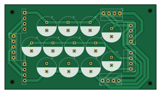
About the Layout PCB
Layout is an open source PCB design by powsplatboom, published on GitHub. It is a 2-layer board measuring 139.7 × 78.7 mm, with 19 components from 7 distinct parts.
By type, the board carries 12 capacitors, 5 connectors and 2 diodes.
It belongs with the audio designs in this gallery.
From the project
Where I will be collecting documentation for all my synth parts
I recommend against building a DIY power supply. That being said, I have built this modular DIY power supply that produces bipolar +/-12VDC and +5VDC. Very low noise, and relatively high current handling. This is the supply I am currently using in my DIY modular rig.
Layout bill of materials (BOM)
19 components, 7 distinct parts — part numbers from the project's BOM.
| Qty | Part | Footprint | Refs |
|---|---|---|---|
| 1 | CONN_02X08_ODD_EVEN Transformer Outputs | TerminalBlock_MetzConnect_Type011_RT05505HBWC_1x05_P5.00mm_Horizontal | J1 |
| 4 | PJ301_THONKICONN Conn_01x04_Male | TerminalBlock_MetzConnect_Type011_RT05504HBWC_1x04_P5.00mm_Horizontal | J2, J3, J4, J5 |
| 2 | B5819W GBU8A | Diode_Bridge_Vishay_GBU | D1, D2 |
| 4 | 10U 10000uf | CP_Radial_D18.0mm_P7.50mm | C1, C2, C3, C4 |
| 3 | 100N 10000uf | CP_Radial_D18.0mm_P7.50mm | C5, C6, C12 |
| 3 | 100P 10000uf | CP_Radial_D18.0mm_P7.50mm | C7, C10, C11 |
| 2 | 0.33U 10000uf | CP_Radial_D18.0mm_P7.50mm | C8, C9 |
Layout design files
The KiCad project lives in the powsplatboom/Synth-DIY repository on GitHub; these links point at the commit this page was built from.
Layout: common questions
How big is the Layout PCB?
The Layout measures 139.7 × 78.7 mm, has 2 copper layers and is 1.6 mm thick.
How many components are on the Layout?
19 components, from 7 distinct parts, with part numbers taken from the project's own BOM. The full bill of materials is listed on this page.
Where can I download the Layout design files?
From the powsplatboom/Synth-DIY repository on GitHub, which has the KiCad layout and the BOM; the links under Design files point to each one.
Can I use the Layout design in my own project?
The repository has no license, so all rights stay with powsplatboom. Use it as a reference, and ask the author before reusing the design.
More boards in Synth-DIY
Panning Mixer
243.8 × 100 mm633 parts4LNo license11
Spring Reverb
170 × 100 mm313 parts4LNo license11
Utility board
399.8 × 72 mm242 parts2LNo license11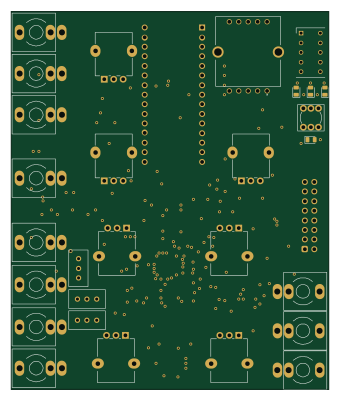 AVR/Arduino
SSI2130 Oscillator
84 × 100 mm185 parts4LNo license11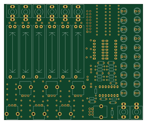
Stereo Mixer
120 × 100 mm121 parts2LNo license11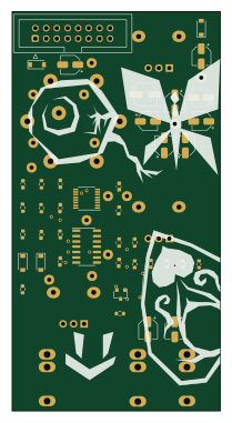
Feed Forward Compressor
49.5 × 95 mm49 parts2LNo license11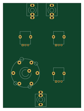
Feed Forward Compressor 14HP
71.1 × 95 mm45 parts2LNo license11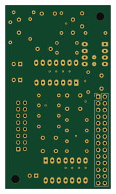
OutputBoard
40 × 70 mm35 parts2LNo license11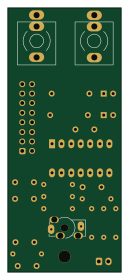
BIGRIG OUTPUT
30 × 70 mm25 parts2LNo license11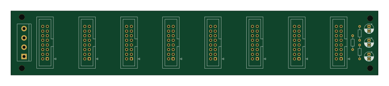
Distribution Board
200 × 35 mm15 parts2LNo license11
Similar boards
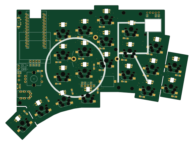
KLOR
GEIGEIGEIST
160.2 × 118.3 mm79 parts2LGPL-3.01.2k
ButtonsLEDs
shanteacontrols
390 × 37 mm82 parts2LApache-2.0956
USB
52 × 12.6 mm6 parts2LApache-2.0956
Pots
390 × 93 mm75 parts2LApache-2.0956
PicoGUS Hand386
polpo
29.2 × 75.2 mm43 parts4LGPL-2.0800
Snark barker
schlae
231.1 × 106.7 mm193 parts2LNo license687