
Powerbank

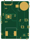
About the Powerbank PCB
Powerbank is an open source PCB design by pranavrasam001-tech, published on GitHub. It is a 2-layer board measuring 31.6 × 42.6 mm, with 19 components from 17 distinct parts.
Other key parts include the TP4056-42-ESOP8, DW01A and MIC2290YML. By type, the board carries 7 resistors, 3 ICs, 3 capacitors, 2 transistors, 1 connector and 1 battery holder.
It belongs with the power & battery designs in this gallery.
From the project
I designed this Mini Power Bank PCB using KiCad to understand how a lithium-ion battery charging and power management circuit is designed from scratch. The board combines a TP4056 charging circuit, a DW01A battery protection circuit, and a MIC2290 boost converter to provide a nom
I designed this Mini Power Bank PCB using KiCad to understand how a lithium-ion battery charging and power management circuit is designed from scratch. The board combines a TP4056 charging circuit, a DW01A battery protection circuit, and a MIC2290 boost converter to provide a nominal 5V output.
The design focuses on battery charging, protection, and voltage conversion without using a microcontroller. I worked on the schematic, component footprint assignment, PCB placement, routing, and preparation of manufacturing files.
Main components on the Powerbank
Powerbank bill of materials (BOM)
19 components, 17 distinct parts — part numbers from the project's BOM.
| Qty | Part | Footprint | Refs |
|---|---|---|---|
| 1 | TP4056-42-ESOP8 TOPPOWER(Nanjing Extension Microelectronics) | SOIC-8-1EP_3.9x4.9mm_P1.27mm_EP2.41x3.3mm_ThermalVias | U1 |
| 1 | DW01A PUOLOP | SOT-23-6 | U2 |
| 1 | MIC2290YML MIC2290 Microchip Tech | Micrel_MLF-8-1EP_2x2mm_P0.5mm_EP0.8x1.3mm_ThermalVias | U3 |
| 2 | FS8205A Q_NMOS_GSD FUXINSEMI | SOT-23-6 | Q1, Q2 |
| 1 | TYPE-C-31-M-12 USB_C_Receptacle_PowerOnly_6P Korean Hroparts Elec | USB_C_Receptacle_HRO_TYPE-C-31-M-12 | J1 |
| 1 | 3000 Battery_Cell Keystone | BatteryHolder_Keystone_3000_1x12mm | BT1 |
| 1 | LTST-C191TBKT LED Lite-On | LED_0603_1608Metric | D1 |
| 1 | SRR1260-100M 10µH BOURNS | L_Bourns_SRR1260 | L1 |
| 1 | C9900011780 2.2µF JLCPCB Assembly | C_0603_1608Metric | C1 |
| 1 | C9900276340 22µF JLCPCB Assembly | C_0805_2012Metric | C2 |
| 1 | CC0603KRX7R9BB104 100nF YAGEO | C_0603_1608Metric | C3 |
| 2 | 0603WAF5101T5E 5.1k UNI-ROYAL(Uniroyal Elec) | R_0603_1608Metric | R1, R2 |
| 1 | 0603WAF2201T5E 2.2k UNI-ROYAL(Uniroyal Elec) | R_0603_1608Metric | R3 |
| 1 | 0603WAF1201T5E 1.2 kΩ UNI-ROYAL(Uniroyal Elec) | R_0603_1608Metric | R4 |
| 1 | 0603WAF1502T5E 15k UNI-ROYAL(Uniroyal Elec) | R_0603_1608Metric | R5 |
| 1 | 0603WAF4991T5E 4.99k UNI-ROYAL(Uniroyal Elec) | R_0603_1608Metric | R6 |
| 1 | 0603WAF1000T5E 100Ω UNI-ROYAL(Uniroyal Elec) | R_0603_1608Metric | R7 |
Powerbank design files
The KiCad project lives in the pranavrasam001-tech/powerbank repository on GitHub; these links point at the commit this page was built from.
Powerbank: common questions
How big is the Powerbank PCB?
The Powerbank measures 31.6 × 42.6 mm, has 2 copper layers and is 1.6 mm thick.
How many components are on the Powerbank?
19 components, from 17 distinct parts, with part numbers taken from the project's own BOM. The full bill of materials is listed on this page.
Where can I download the Powerbank design files?
From the pranavrasam001-tech/powerbank repository on GitHub, which has the KiCad layout, the schematic and the BOM; the links under Design files point to each one.
Can I use the Powerbank design in my own project?
The repository has no license, so all rights stay with pranavrasam001-tech. Use it as a reference, and ask the author before reusing the design.
Similar boards
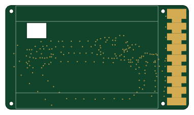
EinkPDA screen
TalismanDesign
95 × 54 mm27 parts2LApache-2.02.0k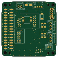
Stack chan
stack-chan
50 × 50 mm33 parts2LApache-2.01.7k
Display Carrier
AxxAxx
35.6 × 58.2 mm5 parts2LGPL-3.01.7k
ProgrammingAdapter
stuartpittaway
10.5 × 83 mm3 parts2LCC-BY-NC-4.01.1k
TemperaturePCB PANEL
116 × 75.5 mm178 parts2LCC-BY-NC-4.01.1k
Module 16S PassiveBalanceAddOn
61 × 74 mm86 parts2LCC-BY-NC-4.01.1k