
Gp ctrl

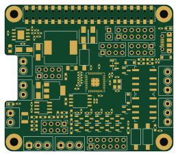
About the Gp ctrl PCB
Gp ctrl is an open source RP2040/RP2350 PCB design by RunLit, published on GitHub under the GPL-3.0 license. It is a 2-layer board measuring 65 × 56.5 mm, with 124 components from 48 distinct parts.
Its main chip is the RP2040, from the RP2040/RP2350 family. Other key parts include the INA219AxD, W25Q64JVSSIQ, NCP1117LPST33T3G and MP1584EN-LF-Z. By type, the board carries 41 resistors, 23 capacitors, 19 connectors, 12 transistors, 10 diodes and 5 ICs.
From the project
general purpose control board
Main components on the Gp ctrl
Gp ctrl bill of materials (BOM)
124 components, 48 distinct parts.
| Qty | Part | Footprint | Refs |
|---|---|---|---|
| 1 | INA219AxD | SOIC-8_3.9x4.9mm_P1.27mm | U1 |
| 1 | W25Q64JVSSIQ | SOIC-8_5.23x5.23mm_P1.27mm | U2 |
| 1 | RP2040 | RP2040-QFN-56 | U3 |
| 1 | NCP1117LPST33T3G | SOT-223-3_TabPin2 | U4 |
| 1 | MP1584EN-LF-Z | MP1584EN-LF-Z | U5 |
| 4 | SolderJumper_2_Open | SolderJumper-2_P1.3mm_Open_TrianglePad1.0x1.5mm | A1, A2, A3, A4 |
| 10 | 2N7002P | SOT-23 | Q1, Q3, Q5, Q6, Q7, Q8, Q9, Q10 +2 |
| 2 | IRLML6244 | SOT-23 | Q2, Q4 |
| 1 | 12MHz | Crystal_SMD_3225-4Pin_3.2x2.5mm | Y1 |
| 1 | DNP | PinHeader_1x02_P2.54mm_Vertical | J1 |
| 1 | Conn_02x20_Odd_Even | Samtec_HLE-120-02-xxx-DV-BE_2x20_P2.54mm_Horizontal | J3 |
| 3 | Screw_Terminal_3.5mm | TerminalBlock_4Ucon_1x02_P3.50mm_Horizontal | J4, J19, J20 |
| 4 | 2.54mm | PinHeader_2x04_P2.54mm_Vertical | J5, J6, J7, J9 |
| 1 | DNP | PinHeader_2x06_P2.54mm_Vertical | J8 |
| 4 | 3.5mm | TerminalBlock_4Ucon_1x03_P3.50mm_Horizontal | J10, J11, J12, J13 |
| 2 | DNP | PinHeader_1x03_P2.54mm_Vertical_SMD_Pin1Left | J14, J15 |
| 1 | Conn_02x06_Odd_Even | PinHeader_2x06_P2.54mm_Vertical | J16 |
| 1 | USB_B_Micro | USB_Micro-B_Molex-105017-0001 | J17 |
| 1 | DNF | PinHeader_1x04_P1.00mm_Vertical_SMD_Pin1Left | J18 |
| 3 | SolderJumper_2_Open | power_jumper | JP1, JP2, JP3 |
Show 28 more
| Qty | Part | Footprint | Refs |
|---|---|---|---|
| 2 | Relay_DPDT_Panasonic_AGQ200A4H | Relay_DPDT_Panasonic_AGQ200A4H | K1, K2 |
| 3 | C2689642 | SW_SPST_CK_PTS636_SP43_SMTR | SW1, SW2, SW3 |
| 5 | SS34 | D_SMA | D1, D2, D7, D9, D10 |
| 3 | B5819W SL | D_SOD-123 | D3, D4, D5 |
| 2 | 19-217/GHC-YR1S2/3T | D_0603_1608Metric_Pad1.05x0.95mm_HandSolder | D6, D8 |
| 1 | 15u | L_12x12mm_H6mm | L1 |
| 12 | 100n | R_0402_1005Metric_Pad0.72x0.64mm_HandSolder | C1, C2, C3, C4, C5, C6, C7, C8 +4 |
| 2 | 1u | R_0402_1005Metric_Pad0.72x0.64mm_HandSolder | C12, C13 |
| 1 | 2.2u | L_0402_1005Metric_Pad0.77x0.64mm_HandSolder | C14 |
| 1 | 100n | L_0402_1005Metric_Pad0.77x0.64mm_HandSolder | C15 |
| 2 | 30pF | C_0402_1005Metric_Pad0.74x0.62mm_HandSolder | C16, C17 |
| 2 | 10u | C_0603_1608Metric_Pad1.08x0.95mm_HandSolder | C18, C19 |
| 1 | 22u | C_1206_3216Metric_Pad1.33x1.80mm_HandSolder | C21 |
| 1 | 150pF | R_0402_1005Metric_Pad0.72x0.64mm_HandSolder | C22 |
| 1 | 10u | C_0805_2012Metric_Pad1.18x1.45mm_HandSolder | C23 |
| 4 | 10K | R_0603_1608Metric_Pad0.98x0.95mm_HandSolder | R1, R2, R22, R27 |
| 10 | 100K | R_0603_1608Metric_Pad0.98x0.95mm_HandSolder | R3, R4, R8, R9, R10, R11, R12, R13 +2 |
| 1 | 0.01 | R_1210_3225Metric_Pad1.30x2.65mm_HandSolder | R5 |
| 10 | 10k | R_0402_1005Metric_Pad0.72x0.64mm_HandSolder | R6, R7, R20, R21, R23, R24, R25, R26 +2 |
| 4 | 33K | R_0603_1608Metric_Pad0.98x0.95mm_HandSolder | R16, R17, R18, R19 |
| 2 | 27.4R | R_0402_1005Metric_Pad0.72x0.64mm_HandSolder | R30, R31 |
| 2 | 1K | L_0402_1005Metric_Pad0.77x0.64mm_HandSolder | R32, R33 |
| 1 | 470R | R_0402_1005Metric_Pad0.72x0.64mm_HandSolder | R34 |
| 1 | 510 | R_0402_1005Metric_Pad0.72x0.64mm_HandSolder | R35 |
| 3 | 100K | R_0402_1005Metric_Pad0.72x0.64mm_HandSolder | R36, R39, R41 |
| 1 | 24.9k | R_0402_1005Metric_Pad0.72x0.64mm_HandSolder | R37 |
| 1 | 210k | R_0402_1005Metric_Pad0.72x0.64mm_HandSolder | R38 |
| 1 | 40.2K | R_0402_1005Metric_Pad0.72x0.64mm_HandSolder | R40 |
Gp ctrl design files
The KiCad project lives in the RunLit/gp-ctrl repository on GitHub; these links point at the commit this page was built from.
- Layoutsch/gp-ctrl.kicad_pcb
- Schematicsch/gp-ctrl.kicad_sch
Gp ctrl: common questions
What microcontroller does the Gp ctrl use?
The Gp ctrl is built around the RP2040, from the RP2040/RP2350 family.
How big is the Gp ctrl PCB?
The Gp ctrl measures 65 × 56.5 mm, has 2 copper layers and is 1.6 mm thick.
How many components are on the Gp ctrl?
124 components, from 48 distinct parts. The full bill of materials is listed on this page.
Where can I download the Gp ctrl design files?
From the RunLit/gp-ctrl repository on GitHub, which has the KiCad layout and the schematic; the links under Design files point to each one.
Can I use the Gp ctrl design in my own project?
Yes, under the terms of its GPL-3.0 license, which RunLit chose for the repository.
Can I test firmware for the Gp ctrl without the hardware?
Yes. HardLabs builds a simulation of the board from its netlist and BOM, so you can run and debug RP2040/RP2350 firmware against it before you order a PCB.
Similar boards
 RP2040/RP2350
Open Book Abridged Edition
joeycastillo
85 × 115 mm29 parts2LCC-BY-SA-4.08.1k RP2040/RP2350
Corne
foostan
277.2 × 107.5 mm164 parts2LCC-BY-4.07.7k RP2040/RP2350
Corne
277.2 × 107.5 mm164 parts2LCC-BY-4.07.7k RP2040/RP2350
LogicAnalyzer
gusmanb
57 × 55.2 mm6 parts2LGPL-3.05.0k RP2040/RP2350
Jitx design
55.5 × 65 mm26 parts4LGPL-3.05.0k RP2040/RP2350
Main
google
98 × 71 mm102 parts2LApache-2.02.9k